Hi Maurizio,
Yes, the DEM clock synchronizer circuit will work when using simultaneous mode. One can view the DEM (Dynamic Element Matching) circuit as a separate circuit that provides accurate current division for the 6 MSBs. It is not strictly necessary to have certain frequency relation with bit clock or word select to make it work.
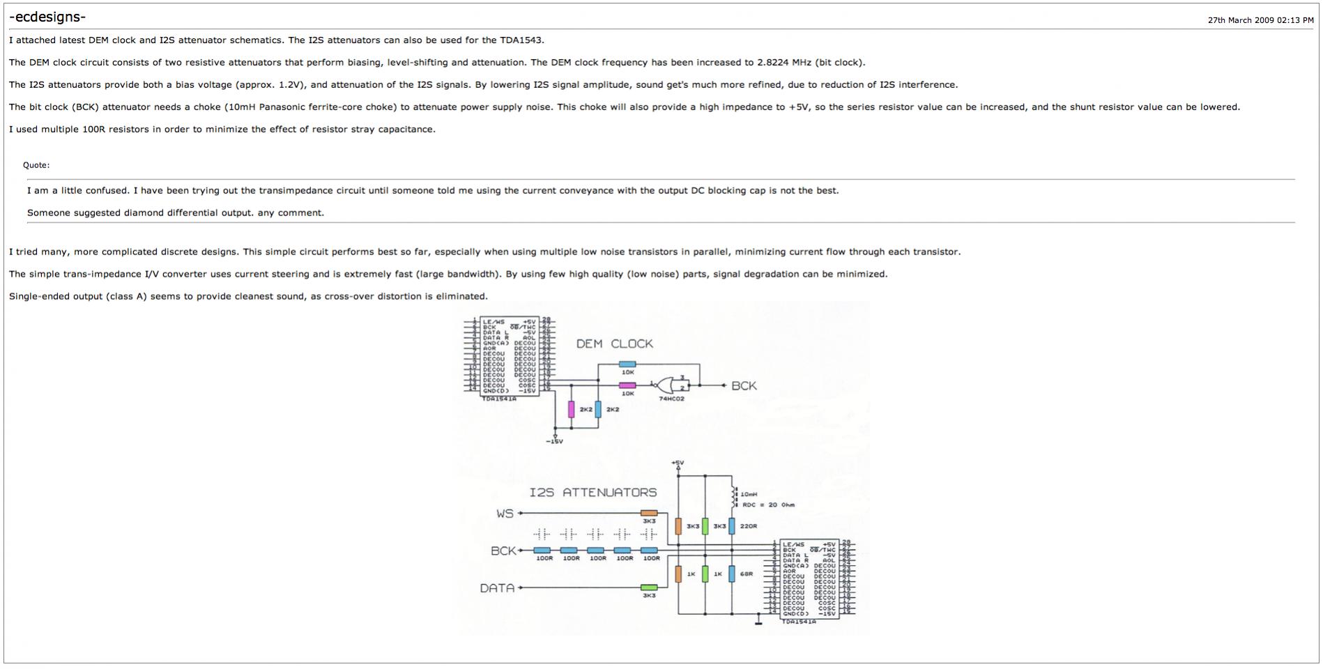
Typical DEM frequency equals 200 KHz, limiting frequency equals 7 Mhz. I have tested applications running on 44.1 KHz DEM clock with 470nF decoupling caps.
You can experiment with bit clock and multiples of the bit clock for the DEM circuit.
With my setup, I achieved best results so far with both 2.8224 MHz bit and DEM clock.
I would like to run it in Simultaneous mode in a Philips 304..
Is it possible to use the DEM from ECDesign for this configuration..?
ECDesign...do you hava any comment or suggestion for me?
Yes, the DEM clock synchronizer circuit will work when using simultaneous mode. One can view the DEM (Dynamic Element Matching) circuit as a separate circuit that provides accurate current division for the 6 MSBs. It is not strictly necessary to have certain frequency relation with bit clock or word select to make it work.
Typical DEM frequency equals 200 KHz, limiting frequency equals 7 Mhz. I have tested applications running on 44.1 KHz DEM clock with 470nF decoupling caps.
You can experiment with bit clock and multiples of the bit clock for the DEM circuit.
With my setup, I achieved best results so far with both 2.8224 MHz bit and DEM clock.
Hi Ryssen,
yes, I have been manufacturing and assembling my own PCBs for over 30 years now.
Next one up is the Cirlotron PCB. PCB design is almost completed, it's a rather large PCB (19 x 19cm) with 3 on-board transformers. I plan to complete a working prototype PCB this week.
You made the pcb´s to?
yes, I have been manufacturing and assembling my own PCBs for over 30 years now.
Next one up is the Cirlotron PCB. PCB design is almost completed, it's a rather large PCB (19 x 19cm) with 3 on-board transformers. I plan to complete a working prototype PCB this week.
Member
Joined 2009
Paid Member
Hi Bigun,I attached a diagram of the stepped attenuator concept (repost).
Hi, thanks very much - I was away the last week on business so just saw your reply to my question.
you explained it perfectly. I like it and it's got me thinking about using it or something similar in my own projects.
Did you consider adding capacitors across each of the diodes to reduce h.f. noise further ?
I'd like to try the syncronous reclocking and DEM clock as shown in post #3465 to my main cd player which uses the old TDA1540D DAC. It's a Revox B225 with TDA7030 (oversampling) IC removed and with a low jitter masterclock fitted. Original oscillator runs at 4.2336Mhz, so I had to use a 8.4672Mhz Tent low jitter followed by a 74hc74 to divide it by two. This clock and and all the 3 tensions feeding the DACs are separately and accurately implemented.
Can someone confirm this operation is possible?
I mainly have 3 doubts:
a) BCK frequency. I believe I should feed it at 1/4 of the master clock = 1.0584Mhz. If I remember correctly in the past I fed 1/4 masterclock (2.88Mhz) directly from the divider on a TDA1541, avoiding direct connection to the decoder IC (oversampling removed). This worked well. But I'm not sure if it can be done with the TDA1540 too.
b) DEM. This is something completely new to me. On the TDA1540 a 820pF capacitor is always used and datasheet reports a 160KHz typical frequency with it a minimum of 100KHz and a max. of 200KHz. I don't know if feeding the BCK through the 74AUC1G74 will generate a suitable signal.
c) as far as I can understand the master clock is fed to the BCK's 74AUC1G74 in order to syncronously reclock it together with WS and DATA lines. Is this right?
Thank you.
Last edited:
Hi fvale,
TDA1540 is a 14 bit mono DAC with external DEM capacitor (pin 8 and 9). The DACs run in 4x oversampling (44,100 * 24 * 4 = 4.2336 MHz bit clock). With NOS the bit clock needs to be divided by 4 resulting in 1.0584 MHz.
The DEM frequency limits (100 ... 200KHz) relate to 820pF external capacitor. It's not the absolute minimum or maximum usable DEM clock range.
I haven't tested the balanced DC-coupled DEM synchronizer on the TDA1540, it might need some adapting (resistor values). It is possible that the TDA1540 like the TDA1541A accepts much higher DEM clock rates. You can start with 176.4 KHz (bit clock divided by 6). Based on max. bit clock frequency (12 MHz) chip circuits should be fast enough to support 1.0584 MHz.
Yes, the 74AUC1G74 synchronously reclocks the 1.0584 MHz bit clock, and both flip-flop outputs (Q and /Q) are used for both, DEM synchronizer and TDA1540 bit clocks. LE and DATA signals of both TDA1540 chips also need to be synchronously reclocked for lowest jitter.
a) BCK frequency. I believe I should feed it at 1/4 of the master clock = 1.0584Mhz. If I remember correctly in the past I fed 1/4 masterclock (2.88Mhz) directly from the divider on a TDA1541, avoiding direct connection to the decoder IC (oversampling removed). This worked well. But I'm not sure if it can be done with the TDA1540 too.
TDA1540 is a 14 bit mono DAC with external DEM capacitor (pin 8 and 9). The DACs run in 4x oversampling (44,100 * 24 * 4 = 4.2336 MHz bit clock). With NOS the bit clock needs to be divided by 4 resulting in 1.0584 MHz.
b) DEM. This is something completely new to me. On the TDA1540 a 820pF capacitor is always used and datasheet reports a 160KHz typical frequency with it a minimum of 100KHz and a max. of 200KHz. I don't know if feeding the BCK through the 74AUC1G74 will generate a suitable signal.
The DEM frequency limits (100 ... 200KHz) relate to 820pF external capacitor. It's not the absolute minimum or maximum usable DEM clock range.
I haven't tested the balanced DC-coupled DEM synchronizer on the TDA1540, it might need some adapting (resistor values). It is possible that the TDA1540 like the TDA1541A accepts much higher DEM clock rates. You can start with 176.4 KHz (bit clock divided by 6). Based on max. bit clock frequency (12 MHz) chip circuits should be fast enough to support 1.0584 MHz.
c) as far as I can understand the master clock is fed to the BCK's 74AUC1G74 in order to syncronously reclock it together with WS and DATA lines. Is this right?
Yes, the 74AUC1G74 synchronously reclocks the 1.0584 MHz bit clock, and both flip-flop outputs (Q and /Q) are used for both, DEM synchronizer and TDA1540 bit clocks. LE and DATA signals of both TDA1540 chips also need to be synchronously reclocked for lowest jitter.
HI EC..
I post the schemes i would like to use..
One is from you..
Please..can you take a look to the other and tell me if is good for a 1541 also..?
In simultaneous mode..the DEM reclock need to created from the Master clock?
THanks...and sorry for my questions..but i've no experience in digital.
Maurizio.
Attachments
Hi all,
Some project updates.
Seems I am coming close to my goal, TDA1541A-MK4 output stage was improved using power MOSFET current buffer, different bias resistors and an extra power supply filter to feed the bias circuit.
All 78XX / 79XX regulators were replaced with fast, high resolution discrete regulator modules. The hybrid coupling cap was also improved by using 2.2uF Monacor MKT, 3.3uF Monacor MKT, and 4u7 Intertechnik tin foil in parallel.
After these mods, the MK4 revealed flaws in my bridge power amp and ALPS volume pot.
The ALPS pot was replaced by a wire wound potentiometer that offers higher resolution and much better performance at lower volume settings.
I built a MOSFET Circlotron power amp to replace the MOSFET bridge power amp, using a breadboard setup for testing. This Circlotron amp uses 2 closely matched power MOSFETs for the differential input driver stage and two more for the Circlotron output stage. The design is fully balanced, this means that power supply noise and hum is effectively attenuated, resulting in no audible noise nor hum, thus maximum clarity. There are only 4 MOSFETs in the power amp signal path, offering very high resolution. The power amp was specifically designed to offer highest reliability and low power consumption. At average listening levels, one monoblock only consumes approx. 14 watts from the mains.
At this resolution, all parts become highly critical, meaning their effect on sound quality becomes clearly audible. I had to use non-inductive wire wound resistors for lowest noise. The conventional bridge rectifier also caused too much switching noise (even with Schottky diodes), so I had to use 3-stage stepped rectifiers. Finally the Circlotron power supply smoothing caps put their "signature" on the sound, introducing the next problem. This problem was fixed with a similar method as used with the hybrid coupling caps.
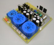
Yesterday I finally completed MOSFET Circlotron power amp PCB lay out and prototype, attached photograph shows the result. It's a single PCB power amplifier, PCB measures 19 x 19cm. The module offers 25 watts rms in 8 Ohms and has a total gain of 30x. The largest part of the PCB space is occupied by the input / driver stage stabilized power supply and both Circlotron output stage power supplies. Both Circlotron output stage power supplies have hybrid smoothing caps that greatly reduce the audible effect of particular electrolytic capacitor types. This results in attenuation of typical capacitor resonance peaks and offer very clean sound. There are multiturn trimmers for DC-offset (this power amp is fully DC-coupled), and bias current. The small transistor to the left of the power MOSFETs acts as a temperature sensor for thermal stabilization. The amplifier was designed such way that loss of power in one or more power supply sections doesn't lead to damaging amplifier nor connected speaker. The stabilized driver stage power supply and temperature sensor provide high bias current stability.
Some project updates.
Seems I am coming close to my goal, TDA1541A-MK4 output stage was improved using power MOSFET current buffer, different bias resistors and an extra power supply filter to feed the bias circuit.
All 78XX / 79XX regulators were replaced with fast, high resolution discrete regulator modules. The hybrid coupling cap was also improved by using 2.2uF Monacor MKT, 3.3uF Monacor MKT, and 4u7 Intertechnik tin foil in parallel.
After these mods, the MK4 revealed flaws in my bridge power amp and ALPS volume pot.
The ALPS pot was replaced by a wire wound potentiometer that offers higher resolution and much better performance at lower volume settings.
I built a MOSFET Circlotron power amp to replace the MOSFET bridge power amp, using a breadboard setup for testing. This Circlotron amp uses 2 closely matched power MOSFETs for the differential input driver stage and two more for the Circlotron output stage. The design is fully balanced, this means that power supply noise and hum is effectively attenuated, resulting in no audible noise nor hum, thus maximum clarity. There are only 4 MOSFETs in the power amp signal path, offering very high resolution. The power amp was specifically designed to offer highest reliability and low power consumption. At average listening levels, one monoblock only consumes approx. 14 watts from the mains.
At this resolution, all parts become highly critical, meaning their effect on sound quality becomes clearly audible. I had to use non-inductive wire wound resistors for lowest noise. The conventional bridge rectifier also caused too much switching noise (even with Schottky diodes), so I had to use 3-stage stepped rectifiers. Finally the Circlotron power supply smoothing caps put their "signature" on the sound, introducing the next problem. This problem was fixed with a similar method as used with the hybrid coupling caps.
Yesterday I finally completed MOSFET Circlotron power amp PCB lay out and prototype, attached photograph shows the result. It's a single PCB power amplifier, PCB measures 19 x 19cm. The module offers 25 watts rms in 8 Ohms and has a total gain of 30x. The largest part of the PCB space is occupied by the input / driver stage stabilized power supply and both Circlotron output stage power supplies. Both Circlotron output stage power supplies have hybrid smoothing caps that greatly reduce the audible effect of particular electrolytic capacitor types. This results in attenuation of typical capacitor resonance peaks and offer very clean sound. There are multiturn trimmers for DC-offset (this power amp is fully DC-coupled), and bias current. The small transistor to the left of the power MOSFETs acts as a temperature sensor for thermal stabilization. The amplifier was designed such way that loss of power in one or more power supply sections doesn't lead to damaging amplifier nor connected speaker. The stabilized driver stage power supply and temperature sensor provide high bias current stability.
Attachments
Hi luxury54
Schematic is in post #3505.
I just added an extra filter between -15V and both 150K bias resistors.
The filter consists of 22 K Ohm and 10mH choke between -15V and both bias resistors. The junction of bias resistors is decoupled to GND using 470uF / 35V Panasonic FM cap. This filter attenuates noise from the -15V rail.
I now use discrete voltage regulators for +5V, -5V, and -15V.
I wonder if you could post the latest TDA1541A output schematic using those power Mosfets and the value of bias resistors for experimental purposes only, Thanks
Schematic is in post #3505.
I just added an extra filter between -15V and both 150K bias resistors.
The filter consists of 22 K Ohm and 10mH choke between -15V and both bias resistors. The junction of bias resistors is decoupled to GND using 470uF / 35V Panasonic FM cap. This filter attenuates noise from the -15V rail.
I now use discrete voltage regulators for +5V, -5V, and -15V.
Regulators
Hi John,
I'd like to know if you are going to sell these regulators (or pcbs) and/or publish the circuit.
Regards Ernst
Hi John,
I now use discrete voltage regulators for +5V, -5V, and -15V.
I'd like to know if you are going to sell these regulators (or pcbs) and/or publish the circuit.
Regards Ernst

Ah, thanks Oliver. I was searching for this thread and only managed to find it again a few minutes ago. It's difficult to find anything as it's so long now.
Just a note, I'm using SAA7220 chip in my transport and outputting i2s into Oliver's dac board design.
Thanks, Lee.
Just a note, I'm using SAA7220 chip in my transport and outputting i2s into Oliver's dac board design.
Thanks, Lee.
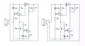
hi ernesternest,
I attached discrete regulator schematics. The circuit on the left is a 78XX replacement (positive output voltage). The one on the right a 79XX replacement (negative output voltage).
Given values are for +5V and -5V output voltage. Output voltage can be changed by changing value of R4 / R9 or voltage of reference L2 / L4.
R3 / R9 set max. output current (lower value gives higher output current). Indicated values provide approx. 250mA max. output current (regulators are short-circuit protected).
The regulators require decoupling caps on both input and output pins, similar as with 78XX and 79XX regulators.
I'd like to know if you are going to sell these regulators (or pcbs) and/or publish the circuit.
I attached discrete regulator schematics. The circuit on the left is a 78XX replacement (positive output voltage). The one on the right a 79XX replacement (negative output voltage).
Given values are for +5V and -5V output voltage. Output voltage can be changed by changing value of R4 / R9 or voltage of reference L2 / L4.
R3 / R9 set max. output current (lower value gives higher output current). Indicated values provide approx. 250mA max. output current (regulators are short-circuit protected).
The regulators require decoupling caps on both input and output pins, similar as with 78XX and 79XX regulators.
Attachments
Hi phi,
The DC output voltage at the volume pot wiper would then vary with volume setting. This in turn would vary bias current in the Circlotron output stage as this is set by the input / driver stage.
So the DAC DC output voltage must be zero. This can be done by using an extra bias voltage that cancels the voltage drop across the I/V resistors (approx. 2V DC). Problem now is that the voltage drops for L and R channels usually differ. This means that there would be still some DC voltage on one of the outputs.
Suppose the full DC-coupling works fine, there is a catch. If the I2S stream to the DAC stops for some reason, the TDA1541A latches last sample and outputs DC voltage during the time there is no I2S stream. This leads to (fatal) DC voltage at the speaker.
This could be solved by a fast DC protection, but that would require a relay contact in series with the speaker and that affects sound quality (switch varying contact resistance). Possible option would be shutting down Circlotron power supply, this takes approx. 2 ... 3 seconds.
When you do such an 'integrated solution' like you do, combining DAC and Poweramp. Wouldn't it be more 'optimal' skipping the coupling cap(s) after the DAC and adapt the powerstage to handle the DC offset from the DAC?
The DC output voltage at the volume pot wiper would then vary with volume setting. This in turn would vary bias current in the Circlotron output stage as this is set by the input / driver stage.
So the DAC DC output voltage must be zero. This can be done by using an extra bias voltage that cancels the voltage drop across the I/V resistors (approx. 2V DC). Problem now is that the voltage drops for L and R channels usually differ. This means that there would be still some DC voltage on one of the outputs.
Suppose the full DC-coupling works fine, there is a catch. If the I2S stream to the DAC stops for some reason, the TDA1541A latches last sample and outputs DC voltage during the time there is no I2S stream. This leads to (fatal) DC voltage at the speaker.
This could be solved by a fast DC protection, but that would require a relay contact in series with the speaker and that affects sound quality (switch varying contact resistance). Possible option would be shutting down Circlotron power supply, this takes approx. 2 ... 3 seconds.
hi ernesternest,
I attached discrete regulator schematics. The circuit on the left is a 78XX replacement (positive output voltage). The one on the right a 79XX replacement (negative output voltage).
Given values are for +5V and -5V output voltage. Output voltage can be changed by changing value of R4 / R9 or voltage of reference L2 / L4.
R3 / R9 set max. output current (lower value gives higher output current). Indicated values provide approx. 250mA max. output current (regulators are short-circuit protected).
The regulators require decoupling caps on both input and output pins, similar as with 78XX and 79XX regulators.
Wow! Thanks, what a gift!
Ernst
some query that came up
John,
I'm now moving from MK4 I/V to MK5 replacing JFets by Fets (BS170 – couldn't find the IRLU120) and adding items, that came along.
How should one set the DC offset by using the added trimmer? Where to measure the offset?
In your most recent I/V scheme beside the usual signal connection via C3 you connect +5V DAC to +15V CIR. Is this mandatory for getting it to work with any amp or just important in combination with the circlotron? Implementation would mean separated ground between DAC and AMP in any case. Is this the reason and advantage?
Regarding the LEDs in your voltage regulators, you specify them to be red. So they are red SMD LEDs. Wonder, if there were further limitations.
Thanks and regards Ernst
Project full schematics
Hi ernesternest,
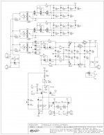
First of all I added latest project schematics as reference:
DAC power supply, TDA1541A-MK5, and Circlotron power amp.
Missing parts are the 10K wire wound volume pot and the 3.3uF V-cap TFTF or hybrid coupling cap.
MK5 schematic shows the MOSFET output circuit in detail. Both C1 and C2 are added to attenuate higher harmonics and residual output glitch, this is necessary to prevent bandwidth problems with attached circuits.
Bias resistors R22 and R23 are connected to an extra RLC filter (R21, N12, and C35). This filter attenuates -15V rail noise. The bias resistors are required to prevent MOSFETs T1 and T2 from switching "off" by ensuring minimum bias current of approx. 70uA.
I suggest to use power MOSFETs like 2SK2391 or 2SK216 for example (there are many more suitable MOSFETs, I even got 2Sk1530 working without problems).
The precision multi turn trimmers P1 and P2 are adjusted for 0V DC between TDA1541A L (pin 25) and GND, and TDA1541A R (pin6) output and GND.
The DAC output voltage appears across passive I/V resistors R3 and R4. In order to tap this ac signal without adding +5V power supply impedance in series with this ac signal, +5V is used as reference instead of GND. tests showed clearly that using +5V as reference performs better.
The fully DC-coupled Circlotron uses combined differential input / driver stage. In order to achieve maximum swing, the gates are connected to +15V and the sources to +20V using 50R trimmer ans approx. 220R resistor. If the gates were tied to GND, I would either need an extra differential (MOSFET) pair, or I would end up with too low output swing.
Viewed from DAC / Circlotron absolute ground references, DAC reference is at +5V and Circlotron input reference is at +15V. When both units are connected together (coupling cap blocks DC) there would be (+15) - (+5) = 10V voltage difference between the GND of both devices. +5V of the DAC is connected to +15V of the Circlotron, but since there is no return path (coupling cap) no DC current can flow between the devices.
Yes they are red (or orange) 1206 size SMD LEDs from Kingbright, they are not critical.
Hi ernesternest,
I'm now moving from MK4 I/V to MK5 replacing JFets by Fets (BS170 – couldn't find the IRLU120) and adding items, that came along.
How should one set the DC offset by using the added trimmer? Where to measure the offset?
First of all I added latest project schematics as reference:
DAC power supply, TDA1541A-MK5, and Circlotron power amp.
Missing parts are the 10K wire wound volume pot and the 3.3uF V-cap TFTF or hybrid coupling cap.
MK5 schematic shows the MOSFET output circuit in detail. Both C1 and C2 are added to attenuate higher harmonics and residual output glitch, this is necessary to prevent bandwidth problems with attached circuits.
Bias resistors R22 and R23 are connected to an extra RLC filter (R21, N12, and C35). This filter attenuates -15V rail noise. The bias resistors are required to prevent MOSFETs T1 and T2 from switching "off" by ensuring minimum bias current of approx. 70uA.
I suggest to use power MOSFETs like 2SK2391 or 2SK216 for example (there are many more suitable MOSFETs, I even got 2Sk1530 working without problems).
The precision multi turn trimmers P1 and P2 are adjusted for 0V DC between TDA1541A L (pin 25) and GND, and TDA1541A R (pin6) output and GND.
In your most recent I/V scheme beside the usual signal connection via C3 you connect +5V DAC to +15V CIR. Is this mandatory for getting it to work with any amp or just important in combination with the circlotron? Implementation would mean separated ground between DAC and AMP in any case. Is this the reason and advantage?
The DAC output voltage appears across passive I/V resistors R3 and R4. In order to tap this ac signal without adding +5V power supply impedance in series with this ac signal, +5V is used as reference instead of GND. tests showed clearly that using +5V as reference performs better.
The fully DC-coupled Circlotron uses combined differential input / driver stage. In order to achieve maximum swing, the gates are connected to +15V and the sources to +20V using 50R trimmer ans approx. 220R resistor. If the gates were tied to GND, I would either need an extra differential (MOSFET) pair, or I would end up with too low output swing.
Viewed from DAC / Circlotron absolute ground references, DAC reference is at +5V and Circlotron input reference is at +15V. When both units are connected together (coupling cap blocks DC) there would be (+15) - (+5) = 10V voltage difference between the GND of both devices. +5V of the DAC is connected to +15V of the Circlotron, but since there is no return path (coupling cap) no DC current can flow between the devices.
Regarding the LEDs in your voltage regulators, you specify them to be red. So they are red SMD LEDs. Wonder, if there were further limitations.
Yes they are red (or orange) 1206 size SMD LEDs from Kingbright, they are not critical.
Attachments
Last edited:
Thanks John for answers and all the circuits!
A preliminary final question I do still have. Have you got a hint for R9 to get -15 V out of your 7915 replacement circuit.
I'm going to order the few new parts I'll need and try to create a layout for the regulators. Some of the parts will be difficult to get, but I think it will be worth trying. Thanks again! Due to Christmas and vacation January will come before a serious result can be seen, heard and maybe shown.
Ernst
- Home
- Source & Line
- Digital Line Level
- Building the ultimate NOS DAC using TDA1541A