Hi EUVL,
with 2SK1530 I measured 0.6 Ohms output impedance with 150mA bias current and no global feedback.
The straight-forward 4-FET design is possible because of the relatively low 2SK1530 MOSFET input capacitance of only 700pF.
The 2SK3497 has specified 2500pF input capacitance (and 5000pF for two in parallel). This would require an extra balanced driver stage, adding at least two extra semiconductors that would further reduce resolution.
Possible alternative for the power MOSFETs could be Silicon Carbide power JFETS from SemiSouth with specified rdsON of 0.15 Ohms and around 600pF input capacitance.
As shown, the output impedance in balanced mode is 2x (1/Yfs) of 2SK1530, which will be around 1 ohm at 2A bias. For me rather too high. I suggest you look into devices like 2SK3497, maybe 2x parallel at 1A bias each, per circlotron side.
with 2SK1530 I measured 0.6 Ohms output impedance with 150mA bias current and no global feedback.
The straight-forward 4-FET design is possible because of the relatively low 2SK1530 MOSFET input capacitance of only 700pF.
The 2SK3497 has specified 2500pF input capacitance (and 5000pF for two in parallel). This would require an extra balanced driver stage, adding at least two extra semiconductors that would further reduce resolution.
Possible alternative for the power MOSFETs could be Silicon Carbide power JFETS from SemiSouth with specified rdsON of 0.15 Ohms and around 600pF input capacitance.
Maybe you have forgotten that in follower mode, only Cgd counts, which is 100pF fpr 2SK1530, and 30pF for 2SK3497.
SemiSouth has about 100pF Cgd, and similar transconductance at low bias to 2SK1530.
For me output impedance too high.
Rdson has no meaning in follower mode.
Patrick
SemiSouth has about 100pF Cgd, and similar transconductance at low bias to 2SK1530.
For me output impedance too high.
Rdson has no meaning in follower mode.
Patrick
Hi EUVL
Yes, seems I forgot this. I will test the 2SK3497 if I can source them without having to buy 100pcs.
There were some problems with the Circlotron prototype, two 2SJ109 JFETs blew-up (gate-source breakdown of the JFET connected to the input). I suspect limited breakdown voltage of 25 ... 30V.
Afterwards I am glad this happened as I put 200V, high Yfs power MOSFETs in the input / driver stage to prevent this from happening again.
The input capacitance is slightly higher (120pF) compared to the 2SJ109 (95pF). Yfs is specified at 35 (typical), 2SJ109 is specified at 22.
However, the perceived sound quality was cleaner and "stress-free" compared to the 2SJ109.
Main reason for me to test power JFETs is the resulting perceived sound quality. Devices that provide similar output impedance can still sound very different.
Maybe you have forgotten that in follower mode, only Cgd counts, which is 100pF fpr 2SK1530, and 30pF for 2SK3497.
Yes, seems I forgot this. I will test the 2SK3497 if I can source them without having to buy 100pcs.
There were some problems with the Circlotron prototype, two 2SJ109 JFETs blew-up (gate-source breakdown of the JFET connected to the input). I suspect limited breakdown voltage of 25 ... 30V.
Afterwards I am glad this happened as I put 200V, high Yfs power MOSFETs in the input / driver stage to prevent this from happening again.
The input capacitance is slightly higher (120pF) compared to the 2SJ109 (95pF). Yfs is specified at 35 (typical), 2SJ109 is specified at 22.
However, the perceived sound quality was cleaner and "stress-free" compared to the 2SJ109.
SemiSouth has about 100pF Cgd, and similar transconductance at low bias to 2SK1530.
For me output impedance too high.
Main reason for me to test power JFETs is the resulting perceived sound quality. Devices that provide similar output impedance can still sound very different.
Hi all,
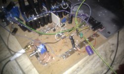
Today i was at John's house hearing the first tones of his new designed Circlotron amp in experimental stage. Look at the attachment.
It's not finished yet. There are still some variables and design philosophies to try. What you see is one channel.
After some listening it is clear to me that this amp has a really great control ability. i only heard this with digital amp's. This aspect is truly amazing! and i think a novum in SS-amp world. While the signal pad is so short without any signal capacitor the resolution is also very, very good. The flavour of sound is tube like, but with lots more power. The high tones could be more brilliant as tubes. We discussed about that and it's possible influenced by the type of PS-capacitors. John uses Panasonic FM at the moment. I prefer Nichicon Gold Tunes. What's next is to try a tube driver instead of SS to get some more 'tube magic'
This amp design is very promising..
Attachments
Hi EUVL,
Digikey hasn't got 100pcs in stock, estimated delivery is in January 2011.
2SK3497 has higher Yfs compared to the 2SK1530, this should lower output impedance, but it also increases local negative feedback. The increased negative feedback could result in more sterile sound.
This conflicts with the principle of fewest possible semiconductors in the signal path. I managed to reduce total amount of semiconductors in the signal path to only 4. This is the minimum amount of components required to construct a balanced bridge amplifier with a gain of 30.
For some reason, low wattage JFETS / MOSFETs in the input / driver stage seem to lead to reduced perceived sound quality. I am now using P-MOSFETs (TO-220 package) with rated 1.75 watts and Yfs of 35 that are designed for audio and video amplifier applications.
You can start a GB for 2SK3497, and 100 pcs will be gone by the end of the day.
You can count me in for 20.
Digikey hasn't got 100pcs in stock, estimated delivery is in January 2011.
2SK3497 has higher Yfs compared to the 2SK1530, this should lower output impedance, but it also increases local negative feedback. The increased negative feedback could result in more sterile sound.
In my design, I cascode the 2SJ109 with J174s. Worth a try. You can also use ZVN3310 with a zener at the gate.
This conflicts with the principle of fewest possible semiconductors in the signal path. I managed to reduce total amount of semiconductors in the signal path to only 4. This is the minimum amount of components required to construct a balanced bridge amplifier with a gain of 30.
For some reason, low wattage JFETS / MOSFETs in the input / driver stage seem to lead to reduced perceived sound quality. I am now using P-MOSFETs (TO-220 package) with rated 1.75 watts and Yfs of 35 that are designed for audio and video amplifier applications.
Reducing the number of the semiconductors in the signal path (hopefully down to zero) is the right direction. I'm sure that at the end John will rediscover the vacuum tubes as he did with the 1 DAC chip vs 8/16 such.
John, please give a chance to the good old 6N6P (6Н6П) even in Class A - Troels already rediscovered them (TRAM w.) or try something like ECC81. The tubes have no thermal (resentful) memory...
John, please give a chance to the good old 6N6P (6Н6П) even in Class A - Troels already rediscovered them (TRAM w.) or try something like ECC81. The tubes have no thermal (resentful) memory...
Hi brubeck,
When you visited me, Circlotron design wasn't completed, in fact I removed some components during experimenting (capacitance multiplier caps) and these weren't put back when you listened to the Circlotron. I also used some bulk metal foil resistors for experimenting that turned out to degrade performance.
But worst of all, the power supplies missed what now turned out to be the the most important circuit in the entire power amplifier.
Circuit performance depends heavily on power supply quality, regardless of how well a circuit is designed. Most important with Circlotron power supply is the use two truly floating power supplies with minimum stray capacitance between both power supplies.
I had to find out the hard way that plain semiconductor rectifiers are basically unusable for high performance designs as they dump switching interference on the connected circuit. This interference consist of pulses with a fundamental frequency of 50, 60, 100, or 120 Hz plus higher harmonics that cover the audio spectrum. The effect of this interference is a muddy "nervous" sound and a background that isn't black.
What happens is that peak charge currents occur, every time the rectifier suddenly starts conducting, and that back emf pulses occur (transformer) when the rectifier suddenly stops conducting and the transformer winding is essentially being disconnected while the voltage hasn't reached zero. Schottky diodes won't solve this specific problem.
The peak charge current is affected by smoothing cap ESR, thus caps with very low ESR will result in highest peak charge currents and highest switching interference levels. Theoretically, low ESR caps should lead to poorer sound quality as they produce higher interference levels when used in a conventional power supply circuit. Capacitors with higher ESR would perform better here as peak charge current would be lower, thus interference levels would be lower.
Unfortunately, circuits perform best when the power supply impedance is as low as possible. Here low ESR (Equivalent Series Resistance) helps.
In practice, the capacitor that offers best balance between impedance and switching interference would offer best sonic performance. Capacitor "rolling" can lead to acceptable performance in a specific application, but it cannot fix this fundamental flaw in power supply rectifier and smoothing circuits. Note that once the interference is generated it's virtually impossible to fully remove it.
Some time ago I published the stepped rectifier concept. It's a simple cheap circuit consisting of some diodes and resistors.
Here the charge current is both, increased and decreased step-wise. This is done by using diode threshold voltage in combination with specific series resistor value. The diode forms an electronic switch that puts the resistor in the current path (diode does not conduct), or bypasses it (diode conducts) as the primary voltage rises. Multiple diode-resistor switches can be placed in series to control the charge and discharge curve. This way the problem is tackled right at the source, by minimizing switching interference.
Now it's no problem to use very low ESR caps while keeping switching interference levels very low.
Yesterday I installed stepped rectifiers on all Circlotron power supplies (including driver stage power supply). I put switches on these stepped rectifiers to bypass them for comparison. With the stepped rectifiers disabled (short circuit) the perceived sound quality is already very high. When the switches are opened, the last bits of "stress", harshness and grain completely vanish, and the sound becomes very realistic. Compare it with listening to music in a room with all kinds of background noises vs a dead quiet room.
First I plan to complete Circlotron MK1 PCB design, the stepped rectifier mod had such impact that I am quite happy with the results of this all-MOSFET design.
We discussed about that and it's possible influenced by the type of PS-capacitors. John uses Panasonic FM at the moment. I prefer Nichicon Gold Tunes. What's next is to try a tube driver instead of SS to get some more 'tube magic'
When you visited me, Circlotron design wasn't completed, in fact I removed some components during experimenting (capacitance multiplier caps) and these weren't put back when you listened to the Circlotron. I also used some bulk metal foil resistors for experimenting that turned out to degrade performance.
But worst of all, the power supplies missed what now turned out to be the the most important circuit in the entire power amplifier.
Circuit performance depends heavily on power supply quality, regardless of how well a circuit is designed. Most important with Circlotron power supply is the use two truly floating power supplies with minimum stray capacitance between both power supplies.
I had to find out the hard way that plain semiconductor rectifiers are basically unusable for high performance designs as they dump switching interference on the connected circuit. This interference consist of pulses with a fundamental frequency of 50, 60, 100, or 120 Hz plus higher harmonics that cover the audio spectrum. The effect of this interference is a muddy "nervous" sound and a background that isn't black.
What happens is that peak charge currents occur, every time the rectifier suddenly starts conducting, and that back emf pulses occur (transformer) when the rectifier suddenly stops conducting and the transformer winding is essentially being disconnected while the voltage hasn't reached zero. Schottky diodes won't solve this specific problem.
The peak charge current is affected by smoothing cap ESR, thus caps with very low ESR will result in highest peak charge currents and highest switching interference levels. Theoretically, low ESR caps should lead to poorer sound quality as they produce higher interference levels when used in a conventional power supply circuit. Capacitors with higher ESR would perform better here as peak charge current would be lower, thus interference levels would be lower.
Unfortunately, circuits perform best when the power supply impedance is as low as possible. Here low ESR (Equivalent Series Resistance) helps.
In practice, the capacitor that offers best balance between impedance and switching interference would offer best sonic performance. Capacitor "rolling" can lead to acceptable performance in a specific application, but it cannot fix this fundamental flaw in power supply rectifier and smoothing circuits. Note that once the interference is generated it's virtually impossible to fully remove it.
Some time ago I published the stepped rectifier concept. It's a simple cheap circuit consisting of some diodes and resistors.
Here the charge current is both, increased and decreased step-wise. This is done by using diode threshold voltage in combination with specific series resistor value. The diode forms an electronic switch that puts the resistor in the current path (diode does not conduct), or bypasses it (diode conducts) as the primary voltage rises. Multiple diode-resistor switches can be placed in series to control the charge and discharge curve. This way the problem is tackled right at the source, by minimizing switching interference.
Now it's no problem to use very low ESR caps while keeping switching interference levels very low.
Yesterday I installed stepped rectifiers on all Circlotron power supplies (including driver stage power supply). I put switches on these stepped rectifiers to bypass them for comparison. With the stepped rectifiers disabled (short circuit) the perceived sound quality is already very high. When the switches are opened, the last bits of "stress", harshness and grain completely vanish, and the sound becomes very realistic. Compare it with listening to music in a room with all kinds of background noises vs a dead quiet room.
What's next is to try a tube driver instead of SS to get some more 'tube magic'
First I plan to complete Circlotron MK1 PCB design, the stepped rectifier mod had such impact that I am quite happy with the results of this all-MOSFET design.
Last edited:
Hi PyroVeso,
Most designers use lots of semiconductors in their design to improve static performance. Static performance can be verified / measured, and the assumption is made that this leads to better sound quality. This is true to some degree, but when it comes to refinement, these static parameters are of little use.
In order to achieve best tracking, servo systems require lowest possible backlash. Example, a milling machine with worn out gears won't be able to mill accurately despite servo correction mechanism. It can still operate with reasonable accuracy, yet fails to maintain high accuracy. In other words, when backlash increases, smallest movements / positioning is affected first.
Every semiconductor has "electronic backlash" comparable with backlash in a gear system. This "electronic backlash" of a semiconductor determines the smallest voltage fluctuation it can track.
Using many semiconductors in a design increases the risk of increased "electronic backlash" and resulting poorer accuracy / tracking. This is why I attempt to minimize the amount of semiconductors in the signal path as this is the simplest way to ensure lower "electronic backlash".
This is why I use "power" MOSFETs in the combined input / driver stage instead of low wattage JFETs like the 2SJ74 or 2SJ109 for example.
Reducing the number of the semiconductors in the signal path (hopefully down to zero) is the right direction.
Most designers use lots of semiconductors in their design to improve static performance. Static performance can be verified / measured, and the assumption is made that this leads to better sound quality. This is true to some degree, but when it comes to refinement, these static parameters are of little use.
In order to achieve best tracking, servo systems require lowest possible backlash. Example, a milling machine with worn out gears won't be able to mill accurately despite servo correction mechanism. It can still operate with reasonable accuracy, yet fails to maintain high accuracy. In other words, when backlash increases, smallest movements / positioning is affected first.
Every semiconductor has "electronic backlash" comparable with backlash in a gear system. This "electronic backlash" of a semiconductor determines the smallest voltage fluctuation it can track.
Using many semiconductors in a design increases the risk of increased "electronic backlash" and resulting poorer accuracy / tracking. This is why I attempt to minimize the amount of semiconductors in the signal path as this is the simplest way to ensure lower "electronic backlash".
The tubes have no thermal (resentful) memory...
This is why I use "power" MOSFETs in the combined input / driver stage instead of low wattage JFETs like the 2SJ74 or 2SJ109 for example.
Yes, Thanks John, for this "Stepped Rectifier Network" design - such a simple thing that works like a charm!
I used it in the headamp and added a single R-C "snubber" and very much quieter amp. Had same success with 15ETH06s and BYW29 diodes in the power amp even with just the 3 'steps'.
I used it in the headamp and added a single R-C "snubber" and very much quieter amp. Had same success with 15ETH06s and BYW29 diodes in the power amp even with just the 3 'steps'.
...........
This is why I use "power" MOSFETs in the combined input / driver stage instead of low wattage JFETs like the 2SJ74 or 2SJ109 for example.
You tried using or considering the high wattge Jfets like the ones from Semisouth?
Hi fff0,
I need certain amount of gain (Yfs), P-channel FETs, and low input capacitance (gain stage in grounded source configuration). This excludes SemiSouth power JFETs. I am currently using matched 2SJ79 MOSFETs in the Circlotron driver stage.
For utmost transparency, very clean power supplies are required, and I plan to test some discrete (shunt) regulators for this driver stage as well.
There are some interesting developments with the TDA1541A-MK4 output stage. Similar as with the Circlotron driver stage, power MOSFETs also perform much better here. Power MOSFETs can offer lower input impedance (grounded gate buffer), so TDA1541A +/- 25mV output compliance can now be fully met (depending on MOSFET properties). The high power devices also seem to have less problems with thermal memory when running on low power.
The required gate bias voltage is tapped from the powerFET drain using a 250K trimmer. The gate is short-circuited to ground (ac signals) using a 1uF film cap. The very small ac signal that manages to seep through the RC filter causes a very small amount of negative feedback.
The MOSFET buffer offers cleaner sound and more "body" (midrange). The sound (clarity) reminds of tube output stages, but without the usual sound coloration and noise.
You tried using or considering the high wattge Jfets like the ones from Semisouth?
I need certain amount of gain (Yfs), P-channel FETs, and low input capacitance (gain stage in grounded source configuration). This excludes SemiSouth power JFETs. I am currently using matched 2SJ79 MOSFETs in the Circlotron driver stage.
For utmost transparency, very clean power supplies are required, and I plan to test some discrete (shunt) regulators for this driver stage as well.
There are some interesting developments with the TDA1541A-MK4 output stage. Similar as with the Circlotron driver stage, power MOSFETs also perform much better here. Power MOSFETs can offer lower input impedance (grounded gate buffer), so TDA1541A +/- 25mV output compliance can now be fully met (depending on MOSFET properties). The high power devices also seem to have less problems with thermal memory when running on low power.
The required gate bias voltage is tapped from the powerFET drain using a 250K trimmer. The gate is short-circuited to ground (ac signals) using a 1uF film cap. The very small ac signal that manages to seep through the RC filter causes a very small amount of negative feedback.
The MOSFET buffer offers cleaner sound and more "body" (midrange). The sound (clarity) reminds of tube output stages, but without the usual sound coloration and noise.
Hi jameshillj,
I already (had to) use them in the DAC power supply. After hearing the impact on power amplifier supply, I probably never use a conventional rectifier in these kind of circuits again.
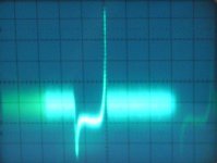
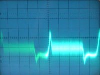
I added an oscillogram to illustrate the effect of a 3-stage stepped rectifier (low, high, full charge current). The voltage is measured across two inches of thin copper wire that is placed between transformer and rectifier.
First picture shows conventional rectifier, setting 10mV/div.
It shows large peak charge current (positive pulse) and a negative pulse caused by transformer back emf.
The second picture shows a 3-stage stepped rectifier added to the same circuit. Both peak charge current and transformer back emf are now reduced, setting 10mV/div.
The stepped rectifier tackles rectifier switching noise right at the source, by doing so it also reduces EMI. Other nice side effect is that the smoothing caps now run cooler so their service life is increased.
Yes, Thanks John, for this "Stepped Rectifier Network" design - such a simple thing that works like a charm!
I already (had to) use them in the DAC power supply. After hearing the impact on power amplifier supply, I probably never use a conventional rectifier in these kind of circuits again.
I added an oscillogram to illustrate the effect of a 3-stage stepped rectifier (low, high, full charge current). The voltage is measured across two inches of thin copper wire that is placed between transformer and rectifier.
First picture shows conventional rectifier, setting 10mV/div.
It shows large peak charge current (positive pulse) and a negative pulse caused by transformer back emf.
The second picture shows a 3-stage stepped rectifier added to the same circuit. Both peak charge current and transformer back emf are now reduced, setting 10mV/div.
The stepped rectifier tackles rectifier switching noise right at the source, by doing so it also reduces EMI. Other nice side effect is that the smoothing caps now run cooler so their service life is increased.
Attachments
Hi fff0,
I need certain amount of gain (Yfs), P-channel FETs, and low input capacitance (gain stage in grounded source configuration). This excludes SemiSouth power JFETs. I am currently using matched 2SJ79 MOSFETs in the Circlotron driver stage.
Opps, I misread, you are referring to driver stage.
Applying this shunt regulator to TDA1541A-MK4's output stage and DAC chip input as well?........
For utmost transparency, very clean power supplies are required, and I plan to test some discrete (shunt) regulators for this driver stage as well.
..........
There are some interesting developments with the TDA1541A-MK4 output stage. Similar as with the Circlotron driver stage, power MOSFETs also perform much better here. Power MOSFETs can offer lower input impedance (grounded gate buffer)........
In Nelson Pass's delite amp, I got the opportunity to check out the difference between IXYS depletion mode Mosfet and Semisouth depletion mode Jfet. Mosfet sounds fuzzy in comparison to say the least. As reported in other thread, I do find that Jfet is more superior in many ways than a mosfet, perhaps due to the lower input capacitance of the Jfet Gate. Yes, High Voltage and bias do better in the amp.
However, I am not sure how will it be applicable to you in TDA1541A-MK4 output stage. Give it a thought?
Last edited:
Member
Joined 2009
Paid Member
Hi Bigun,
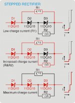
I attached a diagram of the stepped attenuator concept (repost).
The diodes act as (threshold) voltage controlled switches. When the diode doesn't conduct (voltage across it is below threshold voltage) the switch is open. When the diode conducts (voltage across the diode exceeds threshold voltage) the switch is closed.
The diodes marked red in the diagram are conducting and can be viewed as a closed switch. The ones marked black are not conducting and can be viewed as an open switch.
It is important to place the stepped rectifier between the existing (bridge) rectifier and the smoothing cap(s).
back to the diagram,
First sketch shows first step, only diode D1 conducts, this is the diode that's part of the existing (bridge) rectifier. The voltage difference between trafo and smoothing cap is too low for D2 and D3 to conduct. So the current can only flow through R1 (47R) providing lowest charge current.
Second sketch shows second step, the voltage exceeds threshold voltage of one more diode. D3 cannot conduct as there is no bypass resistor, so D2 has to start conducting and creates a second bypass through R2 (10R). This increased charge current is added to the current already flowing through R1. This provides medium charge current.
Third sketch shows third step, the voltage exceeds threshold voltage of both, D2 and D3. Now both, D2 and D3 can conduct, bypassing both R1 and R2. This provides full charge current.
This process takes place within fractions of milliseconds and the resistors only dissipate very little power. When the input voltage drops, the charge current is reduced in a similar way, providing minimum charge current just before all diodes stop conducting. This reduces trafo back emf as can be seen on the oscillograms in post #3493.
Resistor values can be adapted to charge current requirements. Higher resistor values for low power applications and lower resistor values for high power applications.
The amount of diode / resistor paths can be increased to provide even smoother charge current control (more intermediate steps).
I think I'm just being a bit 'slow' today, but I'd really like to see a sketch / schematic of this stepped rectifier to understand what you mean by this - it's definitely caught my attention !
I attached a diagram of the stepped attenuator concept (repost).
The diodes act as (threshold) voltage controlled switches. When the diode doesn't conduct (voltage across it is below threshold voltage) the switch is open. When the diode conducts (voltage across the diode exceeds threshold voltage) the switch is closed.
The diodes marked red in the diagram are conducting and can be viewed as a closed switch. The ones marked black are not conducting and can be viewed as an open switch.
It is important to place the stepped rectifier between the existing (bridge) rectifier and the smoothing cap(s).
back to the diagram,
First sketch shows first step, only diode D1 conducts, this is the diode that's part of the existing (bridge) rectifier. The voltage difference between trafo and smoothing cap is too low for D2 and D3 to conduct. So the current can only flow through R1 (47R) providing lowest charge current.
Second sketch shows second step, the voltage exceeds threshold voltage of one more diode. D3 cannot conduct as there is no bypass resistor, so D2 has to start conducting and creates a second bypass through R2 (10R). This increased charge current is added to the current already flowing through R1. This provides medium charge current.
Third sketch shows third step, the voltage exceeds threshold voltage of both, D2 and D3. Now both, D2 and D3 can conduct, bypassing both R1 and R2. This provides full charge current.
This process takes place within fractions of milliseconds and the resistors only dissipate very little power. When the input voltage drops, the charge current is reduced in a similar way, providing minimum charge current just before all diodes stop conducting. This reduces trafo back emf as can be seen on the oscillograms in post #3493.
Resistor values can be adapted to charge current requirements. Higher resistor values for low power applications and lower resistor values for high power applications.
The amount of diode / resistor paths can be increased to provide even smoother charge current control (more intermediate steps).
Attachments
Hi fff0,
Depletion power MOSFET IXTH20N50D:
2500pF input capacitance.
Semisouth power JFET SJEP120R100:
670pF input capacitance.
Input capacitance (670 ... 2500pF) appears across 47K input impedance.
Apart from the lower input capacitance, power JFETs like the SJEP120R100 may offer better linearity.
It's also a single-ended power amplifier that is highly sensitive to power supply noise.
In my application I use the MOSFETs as grounded-gate buffer. The 2Sk216 has 90pF input capacitance and Yfs of 40. The input capacitance (gate-source) appears across a low impedance of around 10 ... 20 Ohms (grounded gate buffer input impedance). The current running through the powerFET is only between 3 and 7 mA. In this application the advantage is the low current running through a powerFET designed to handle much higher power dissipation (30W peak at room temperature for the 2SK216). This reduces the thermal memory effect and provides much cleaner sound compared to devices (JFETs) that are only rated at 200mW.
In Nelson Pass's delite amp, I got the opportunity to check out the difference between IXYS depletion mode Mosfet and Semisouth depletion mode Jfet. Mosfet sounds fuzzy in comparison to say the least. As reported in other thread, I do find that Jfet is more superior in many ways than a mosfet, perhaps due to the lower input capacitance of the Jfet Gate. Yes, High Voltage and bias do better in the amp.
Depletion power MOSFET IXTH20N50D:
2500pF input capacitance.
Semisouth power JFET SJEP120R100:
670pF input capacitance.
Input capacitance (670 ... 2500pF) appears across 47K input impedance.
Apart from the lower input capacitance, power JFETs like the SJEP120R100 may offer better linearity.
It's also a single-ended power amplifier that is highly sensitive to power supply noise.
In my application I use the MOSFETs as grounded-gate buffer. The 2Sk216 has 90pF input capacitance and Yfs of 40. The input capacitance (gate-source) appears across a low impedance of around 10 ... 20 Ohms (grounded gate buffer input impedance). The current running through the powerFET is only between 3 and 7 mA. In this application the advantage is the low current running through a powerFET designed to handle much higher power dissipation (30W peak at room temperature for the 2SK216). This reduces the thermal memory effect and provides much cleaner sound compared to devices (JFETs) that are only rated at 200mW.
Good morning John,
I'm working on a 1541 DAC, built on Olivers (DVB Project) boards, but with some differences. I'm using your MK4 I/V stage and have implemented your stepped rectifiers.
Regarding the stepped rectifiers you mentioned in your last post, the resistor values depend on the application. As far I've seen you've posted two different pictures so far. In one you used 10R and 47R, in an earlier scheme I think I saw 47R and 470R. Is it possible to give a rule of thumb for dimensioning these, lets say depending on the current drawn.
Using Olivers boards as a base, which has implemented an earlier stage of your I2S attenuatuion and DEM reclocking (with 74HC02 or NL17SZ02), I'd like to move forward to your newer design. For both, I2S attenuation and DEM reclocking you are using now 74AU1G74, which I unfortunately cannot find anywhere. Would you mind giving a hint for a source?
Thanks for sharing your your projects here!!!
Regards Ernst
Searching not only for the name but for function brought this:
TEXAS INSTRUMENTS|SN74AUC1G74DCUR|LOGIC, 74AUC1G, D FLIP FLOP, US8 | Farnell Deutschland
Could be the part, couldn't it?
Ernst
TEXAS INSTRUMENTS|SN74AUC1G74DCUR|LOGIC, 74AUC1G, D FLIP FLOP, US8 | Farnell Deutschland
Could be the part, couldn't it?
Ernst
- Home
- Source & Line
- Digital Line Level
- Building the ultimate NOS DAC using TDA1541A