It seems that you're still improving, looking at the recent capacitor discussions.
I used to use a Thel Silver Mica (0,1u) as coupling cap some time ago. It is really close to a piece of wire. (I tried also some other high-end caps - all of them failed in comparision.)
If we talk about ultimate solutions: I am running my Sabre DAC "without coupling caps" directly connected to the amp right now. You'd be surprised. The best cap is no cap!") ( beside that you'll save a hell lot of money)
( beside that you'll save a hell lot of money)
Cheers
I used to use a Thel Silver Mica (0,1u) as coupling cap some time ago. It is really close to a piece of wire. (I tried also some other high-end caps - all of them failed in comparision.)
If we talk about ultimate solutions: I am running my Sabre DAC "without coupling caps" directly connected to the amp right now. You'd be surprised. The best cap is no cap!
( beside that you'll save a hell lot of money)Cheers
If u feed this DC into the amp, will it alter the DC condition of the amp ? Will cause any unexpected / damage to the amp ? Surely it will cause a lot of hum right.
I replace the IV resistor with DALE 1.8k IV and found the transparency even better. This IV resistor is very important. However, I wonder how important is that 500R resistor.
Overall I found the single ended transimpedance to be more neutral, very uncolor.
I replace the IV resistor with DALE 1.8k IV and found the transparency even better. This IV resistor is very important. However, I wonder how important is that 500R resistor.
Overall I found the single ended transimpedance to be more neutral, very uncolor.
Hi ccschua,
Like I mentioned before, Vishay bulk metal foil is basically the only option when utmost transparency and neutrality is preferred.
I have just completed trans-impedance converter tuning for both TDA1543 and TDA1541A.
Bias current appears to have a "sweet spot" around 40uA. This produces most "open" sound and best focus.
Both a current source in series with 15K resistor, or a JFET current source in series with a 15K resistor works fine. The bias current runs from the emitter of T1 to GND (TDA1543), or -15V (TDA1541A). When using the schematic of post #2704, R7, R9, R10, and R11 need to be replaced with 15 K Ohm resistors.
The output buffer works best with a choke in series with the 500 Ohm resistor (I currently use a small modem transformer as choke).
Power supply decoupling is also very important, I now use at least 3000uF (multiple caps in parallel) across every DAC chip power supply (-5V, +5V, and -15V).
Underestimated problem is active divider decoupling cap grounding, it's absolutely NOT allowed to have any other current passing the decoupling cap GND return paths. This will greatly reduce sound quality. Best is to route each of the 12 decoupling cap GND connections straight to TDA1541A pin 5.
The trace length of the decoupling caps is also very important. In order to minimize trace length and capacitor inductance, I plan to use miniature 1210 size 100nF SMD film caps for decoupling.
Same applies for the DAC analogue GND for the I/V converter, use a separate GND connection that goes straight to pin 5, again this GND connection must not share other (supply) currents.
It's the best performing circuit I tested so far, especially after optimizing bias current and adding the choke in the output buffer.
I replace the IV resistor with DALE 1.8k IV and found the transparency even better. This IV resistor is very important. However, I wonder how important is that 500R resistor.
Like I mentioned before, Vishay bulk metal foil is basically the only option when utmost transparency and neutrality is preferred.
I have just completed trans-impedance converter tuning for both TDA1543 and TDA1541A.
Bias current appears to have a "sweet spot" around 40uA. This produces most "open" sound and best focus.
Both a current source in series with 15K resistor, or a JFET current source in series with a 15K resistor works fine. The bias current runs from the emitter of T1 to GND (TDA1543), or -15V (TDA1541A). When using the schematic of post #2704, R7, R9, R10, and R11 need to be replaced with 15 K Ohm resistors.
The output buffer works best with a choke in series with the 500 Ohm resistor (I currently use a small modem transformer as choke).
Power supply decoupling is also very important, I now use at least 3000uF (multiple caps in parallel) across every DAC chip power supply (-5V, +5V, and -15V).
Underestimated problem is active divider decoupling cap grounding, it's absolutely NOT allowed to have any other current passing the decoupling cap GND return paths. This will greatly reduce sound quality. Best is to route each of the 12 decoupling cap GND connections straight to TDA1541A pin 5.
The trace length of the decoupling caps is also very important. In order to minimize trace length and capacitor inductance, I plan to use miniature 1210 size 100nF SMD film caps for decoupling.
Same applies for the DAC analogue GND for the I/V converter, use a separate GND connection that goes straight to pin 5, again this GND connection must not share other (supply) currents.
Overall I found the single ended transimpedance to be more neutral, very uncolor.
It's the best performing circuit I tested so far, especially after optimizing bias current and adding the choke in the output buffer.
-ecdesigns- said:Hi gaetan8888,
Yes this attenuator diagram is ok, use one of these for all DATA and WS signals (you will need 4 of these). Then use two more for BCK, but now using lower resistor values. The VCC of these BCK attenuators are connected to 5V using a 10mH choke, and the 330 Ohm resistor Vcc (that's now connected to the 10mH choke), is decoupled to GND using 1500uF/6.3V. This is very important in order to attenuate 5V power supply noise.
74F00 is a NAND gate and it inverts, you need a NON-inverting buffer like the 74F125 for example. These are also available as a single buffer (Fairchild tiny logic series), but these are SMD.
Also use Damping (series) resistors on both buffer input and buffer output. Experiment with 100 Ohm ... 1 K Ohm.
Hello John
For the BCK (SCK) clock buffer, I only have 74F244 octal buffer, but that chip are a bit different and there is only one comon OE for all buffer inside.
Thank
Bye
Gaetan
Hi EC
For decoupling you may want to try the FCP1913H104J-E3, which I think are identical panasonic ECHU, stacked metallized PPS 50V .1uF. So if I understand it right you run all 14 (not 12) decoupling caps in parallel to a trace and that trace is only connected to pin 5. Is pin 5 connected to GND or left floating? I guess you could setup a sub star GND right at pin 5 and run individual traces directly to the star.
Thanks
JimS
Hi John,
A little off topic question,
I was just curious about how this machine would sound in NOS operation, but after desolder de SAA7220 p/b and reconstruct it's I2S lines ... listening to it reveals noise that drifts in en out of signal.
Is there something in the 'glue logic' I didn't see?
[The thing is mid 1980's technology, TDA1541, SAA7220 Digitale filter and CX23053, exceedingly well build, locks on 32/44.1/48KHz and has a two layer PLL, the first "fast" one in the receiver and a slow one with several seconds as timeconstant (guess from time to lock when signal applied and schematic) following that. The signal then goes to the SAA7220 Digital Filter, Loads of glue logic inbetween too and from there to a reclocker, from the second PLL clock. The main lines to the DAC then pass through Opto-Isolators (pretty good ones!), the whole thing is 16 Bit 4 times oversampling.]
I know I can put in the CS8412 or SAA 7210 receiver and skip the glue and couplers etc.... but I would like to keep it as it is..... and if that's without the possibility of NOS operation .... So be it, I'll put in the SAA7220 back again.
regards,
Anton.
Attachments
Hi ECDesigns,
If I use TDA1541A, how to connect up the charge transfer circuit with the bias current. The charge transfer is floating. I guess all the connection to ground has to be connected to the -ve rail.
also the bias current at 40uA means the resistor is 15V/40u which is 375kohm, am I right.
below is my project board. so far no noise, unless I crank the volume to 3/4.
Hi jims,
Thanks for the tip. It's rather difficult to route a separate GND trace from each of the 14 decoupling caps to pin 5, especially when traces need to be as short as possible (very limited PCB space). So I connect all decoupling cap GND returns of the R channel to pin 5 using a thick trace, same applies for the L channel decoupling caps. This requires only 2 separate GND return paths. I already tested PCB lay-out using 1210 size SMD parts and these will just fit. These capacitors are all mounted underneath the TDA1541A chip to minimize trace length.
It's also possible to use through-hole capacitors with a pitch of 5mm, soldered on the solder side, underneath the TDA1541A. When all caps are closely placed together, it's just possible. So this is another option.
Pin 5 is connected to GND. I plan to provide separate GND pins that must all be connected to an un-interrupted GND plane on the mainboard. I had very good results with this, using the D1 prototype. During TDA1541A module evaluation, I ended-up with a very small module, just slightly larger than the TDA1541A.
I also stumbled upun strange DEM clock oscillator properties. When the DEM clock is tuned to an almost exact multiple of BCK, it automatically locks to BCK, and the DEM clock signal looks perfect (low jitter). I suspect this is caused by on-chip crosstalk between BCK and the DEM clock oscillator circuit.
This method also works with multiple DAC chips, however, it's not guaranteed that the multiple DEM clocks will run in phase, but this doesn't seem to be a problem as they do run in sync with BCK.
Example, I used 220pF (1%) in parallel with 27pF (1%), BCK = 2.8224 MHz, and most of the TDA1541A chips I tested locked on 352.8 KHz. Due to chip tolerances it may be necessary to slightly tune total capacitance (trimmer in parallel with a fixed polystyrene or silvered mica cap).
I was able to lock on the following DEM clock frequencies by changing the DEM clock capacitor to a close match:
282.24 Khz, 313.6 KHz, 352.8 KHz, 403.2 KHz, 470.4 KHz, 564.48 KHz, 705.6 KHz.
I could make a list of the exact DEM clock capacitor value for each of these DEM clock frequencies, these could act as coarse reference for tuning.
This means that the external DEM clock circuit (plus possible interference) is no longer required when the DEM clock capacitor value is accurately tuned to the DAC chip properties. It's best to have a frequency meter and an oscilloscope at hand, in order to verify correct operation.
For decoupling you may want to try the FCP1913H104J-E3, which I think are identical panasonic ECHU, stacked metallized PPS 50V .1uF. So if I understand it right you run all 14 (not 12) decoupling caps in parallel to a trace and that trace is only connected to pin 5. Is pin 5 connected to GND or left floating? I guess you could setup a sub star GND right at pin 5 and run individual traces directly to the star.
Thanks for the tip. It's rather difficult to route a separate GND trace from each of the 14 decoupling caps to pin 5, especially when traces need to be as short as possible (very limited PCB space). So I connect all decoupling cap GND returns of the R channel to pin 5 using a thick trace, same applies for the L channel decoupling caps. This requires only 2 separate GND return paths. I already tested PCB lay-out using 1210 size SMD parts and these will just fit. These capacitors are all mounted underneath the TDA1541A chip to minimize trace length.
It's also possible to use through-hole capacitors with a pitch of 5mm, soldered on the solder side, underneath the TDA1541A. When all caps are closely placed together, it's just possible. So this is another option.
Pin 5 is connected to GND. I plan to provide separate GND pins that must all be connected to an un-interrupted GND plane on the mainboard. I had very good results with this, using the D1 prototype. During TDA1541A module evaluation, I ended-up with a very small module, just slightly larger than the TDA1541A.
I also stumbled upun strange DEM clock oscillator properties. When the DEM clock is tuned to an almost exact multiple of BCK, it automatically locks to BCK, and the DEM clock signal looks perfect (low jitter). I suspect this is caused by on-chip crosstalk between BCK and the DEM clock oscillator circuit.
This method also works with multiple DAC chips, however, it's not guaranteed that the multiple DEM clocks will run in phase, but this doesn't seem to be a problem as they do run in sync with BCK.
Example, I used 220pF (1%) in parallel with 27pF (1%), BCK = 2.8224 MHz, and most of the TDA1541A chips I tested locked on 352.8 KHz. Due to chip tolerances it may be necessary to slightly tune total capacitance (trimmer in parallel with a fixed polystyrene or silvered mica cap).
I was able to lock on the following DEM clock frequencies by changing the DEM clock capacitor to a close match:
282.24 Khz, 313.6 KHz, 352.8 KHz, 403.2 KHz, 470.4 KHz, 564.48 KHz, 705.6 KHz.
I could make a list of the exact DEM clock capacitor value for each of these DEM clock frequencies, these could act as coarse reference for tuning.
This means that the external DEM clock circuit (plus possible interference) is no longer required when the DEM clock capacitor value is accurately tuned to the DAC chip properties. It's best to have a frequency meter and an oscilloscope at hand, in order to verify correct operation.
interesting,
but so far everybody using a separate DEM clock circuit reported Positive changes in sound compared to that existing 470pF/680pF capacitor value specified in the TDA datasheet
another thing dear ECdesigns,
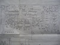
maybe you could point me out what changes should i bring to this schematic posted by you a time ago in order to obtain -5V and not +5V as it is for now
Thanks!
but so far everybody using a separate DEM clock circuit reported Positive changes in sound compared to that existing 470pF/680pF capacitor value specified in the TDA datasheet
another thing dear ECdesigns,
maybe you could point me out what changes should i bring to this schematic posted by you a time ago in order to obtain -5V and not +5V as it is for now
Thanks!
An externally hosted image should be here but it was not working when we last tested it.
ps decoupling on tda1541 pcb
Hi John,
on the tda1541 pcbs, there are 2 x 33uf bypass caps for each of the 3 voltages. I am about to order all of the components for this project - is it worth ordering different values caps and more of them so that i can add them to the pcb, or am i better off sticking with the 33uf bypass caps and try to add some extra smd bypass caps to get up to the 1000uf value that gave the best performance.
Hi scrutinizer,
Could you email me a higher resolution schematic, including the TDA1541 chips and output circuit?
SAA7220 pin 2 (clock input) doesn't seem to receive a clock signal, so when connecting the bit clock input of the TDA1541A to this pin, it won't work. This is probably part of the multiple sample frequency support. Also connect a 2K2 pull-up resistor between SAA7220 pin 2 and Vcc (the removed SAA7220 has an internal pull-up on this pin).
I suggest dividing the crystal clock input signal (SAA7220 pin 11) by 4 using a suitable divider like a 74HC161. Then feed the divided clock signal to the TDA1541 bit clock input.
I was just curious about how this machine would sound in NOS operation, but after desolder de SAA7220 p/b and reconstruct it's I2S lines ... listening to it reveals noise that drifts in en out of signal.
Could you email me a higher resolution schematic, including the TDA1541 chips and output circuit?
SAA7220 pin 2 (clock input) doesn't seem to receive a clock signal, so when connecting the bit clock input of the TDA1541A to this pin, it won't work. This is probably part of the multiple sample frequency support. Also connect a 2K2 pull-up resistor between SAA7220 pin 2 and Vcc (the removed SAA7220 has an internal pull-up on this pin).
I suggest dividing the crystal clock input signal (SAA7220 pin 11) by 4 using a suitable divider like a 74HC161. Then feed the divided clock signal to the TDA1541 bit clock input.
With regards to the transimpedance circuit for TDA1541a, I found replacing the output resistor (after the 4.7uF cap) to different can alter the sound.
At first I use 8k, found less mid but clear high and low. When I change to 150k, the mid is more pronounce. Is it the 8k and the 4.7uF roll off at too high a frequency ?
I notice no matter what I do, the dc offset at the output is minimum 5mV. Is it the 4.7uF pp cap not good ? leaking ?
Hi Luxury54, how is it your TDA1541a doing. Are u trying the floating charge transfer ? I may be thinking to replace the output coupling cap with Mundorf ZN.
hello ccschua,
I'm modding a Marantz player based on TDA1541A now and regarding decoupling capacitors i must say that i found
out a strange thing in a positive way !
The player had originally 14 pieces of 100nF SMD capacitors under the DAC for decoupling and i bypassed them all with 220nF Wima film and the sound wasn't so impressive at that time...
But just doing an experiment and decoupling the last MSB pin with 1uF tantal capacitor and the one near it with 220nF also tantal gave me the sound i was never hoping to obtain just by these capacitor decoupling tweaks
The bass became deeper and softer,the highs became very crisp and there is a slight attenuation of the middle-high range compared to the non polarized film decoupling caps
I love the new sound these caps gave me
Just try it yourself you'll be surprized, but remember since tantal capacitors are polarized and we are dealing with -15V here, you have to solder them with + side to earth and - to TDA pin.
I think i will desolder all of the films and SMD and go with short leg 100nF tantal all the way
ps.
I saw in many schematics/equipment and i don't know if it's a rule,but in general the modules that were powered simultaneously by + and - power rails were always coupled with non-polarized film caps ,and the modules where just one positive power rail was present were always (de)coupled with polarized caps...having this in mind and since only -15V is used in TDA as for this analog part ,i experimented here with polarized tantals and found out that are just great!
soundcheck said:It seems that you're still improving, looking at the recent capacitor discussions.
I used to use a Thel Silver Mica (0,1u) as coupling cap some time ago. It is really close to a piece of wire. (I tried also some other high-end caps - all of them failed in comparision.)
If we talk about ultimate solutions: I am running my Sabre DAC "without coupling caps" directly connected to the amp right now. You'd be surprised. The best cap is no cap!
Cheers
I am building one of Johns 4 x TDA1541 DACS, and am thinking about the best i/v stage. I have been thinking about using Vishay Z foil resistors for the RIV - and even considering those 2 or 3uf V-CAPS - i must be mad at that price, so a balanced output from the DAC certainly appeals.
Does anyone have any schematics/ details regarding the trans impedance/ I/V stage for the 4 x TDA1541 DAC, WITH balanced output? please?
Brad
-ecdesigns- said:Hi scrutinizer,
Could you email me a higher resolution schematic, including the TDA1541 chips and output circuit?
SAA7220 pin 2 (clock input) doesn't seem to receive a clock signal, so when connecting the bit clock input of the TDA1541A to this pin, it won't work. This is probably part of the multiple sample frequency support. Also connect a 2K2 pull-up resistor between SAA7220 pin 2 and Vcc (the removed SAA7220 has an internal pull-up on this pin).
I suggest dividing the crystal clock input signal (SAA7220 pin 11) by 4 using a suitable divider like a 74HC161. Then feed the divided clock signal to the TDA1541 bit clock input.
Hi John,
Thanks for your time and advice!
I found the culprit, John ..... One of the opto-couplers sending word select to the TDA1541a/S1 was unstable due to a 'old' solder joint gone bad over time.
After reparing and tweaking the lowpass .... the sound was not bad at all from this oldtimer.
I possess also the CD 94, maybe it's a nice idea to turn that into a transport only (cdm 1), providing I2S to the CDA 94........

rgds,
Anton.
Hi luxury54,
TDA1541A LSB current change equals 0.004 / 65536 = 61nA.
Active divider decoupling caps are directly connected between divider output and GND, so the slightest decoupling cap leakage current will change exact output current of 6 MSBs!
Typical tantalium cap leakage current (0.1uF ... 1uF) equals 500nA, so this will introduce up to 3-bit error on each of the MSBs. Leakage current also changes with other external factors like temperature and voltage. The tantalium caps should be ok for power supply decoupling.
Ceramic capacitors are microphonic (they will produce a small voltage when tapped, and will flex when a voltage is applied). High-K ceramic caps can produce audible sound when driven by a bias voltage with a super-imposed 1KHz sinewave for example. This makes them less suitable for audio applications.
The active divider decoupling caps do have clearly audible effect on sound quality. The decoupling caps need to have low inductance, very low leakage current, and low microphonics. Some of the active divider outputs have only half the ripple frequency (check TDA1540 datasheet), and the ripple currents vary with the output current.
So capacitors filtering fDEM / 2 need to have twice the capacity of the capacitor filtering fDEM. fDEM is typically around 200 KHz. Capacitors filtering lower currents also have lower ripple current to filter, so capacitance can also be lower. When selecting capacitor values with respect to DEM clock ripple current frequency and active divider output current, and using 1uF as maximum value, following would apply:
pin 13,18, 2mA, fDEM /2, 1uF
pin 12,19, 1mA, fDEM, half current (13,18), twice the frequency of MSB, 250nF
pin 11,20, 0.5mA, fDEM / 2, half frequency, half current (12,19), 125nF
pin 10,21, 0.25mA, fDEM, half current double frequency (11,20), 31.25nF
pin 9,22, 0.125mA, fDEM / 2, half current, half frequency (10,21), 31.25nF
pin 8,23, 0.0625mA, fDEM, half current (9,22), 7,8nF
pin 7,24, 0.0625mA, fDEM, equal current (8,23), 7.8nF.
In practice, 1uF (MSB), 220nF, 120nF, 33nF, 33nF, 8.2nF, 8.2nF. This would give equal ripple currents on all MSBs.
Active divider decoupling also depends on DEM clock. Like mentioned before, DEM clock oscillator is able to "lock" on (on-chip) BCK crosstalk. By selecting DEM clock capacitor values that produce (almost) exact multiples of fs, the DEM clock will "lock" to BCK and jitter amplitude would drop significantly. The often used 470pF and 680pF won't result in a "lock" and produce maximum DEM clock jitter amplitude.
Here are some capacitor values that result in a "lock" condition, capacitance might vary slightly due to TDA1541A tolerances:
235.2 KHz, 350pF
256.58181 KHz, 318pF
282.24 KHz, 300pF
313.6 KHz, 260pF
352.8 KHz, 250pF
403.2 KHz, 203pF
470.4 KHz, 180pF
564.48 KHz, 145pF
705.6 KHz, 122pF
The capacitors need to have tight tolerance (1%).
Today I tested a new (more stable) external DEM clock circuit. It consists of a differential TTL-level clock source (352.8 or 705.6 KHz), and 4 resistors. each DEM clock pin (16 & 17) is connected to -15V through a 2K2 resistor. The TTL-level clock signals are connected to pin 16 & 17 using 10K Ohm series resistors. The resistors will provide bias voltage (prevents the internal DEM clock from oscillating), attenuation and level conversion. This is the best performing DEM clock circuit so far.
DEM clock operation must be tested with low level recordings (-40dB for example). Sheffield test CD "My Disc" contains such test tracks. When the DEM clock doesn't work, there is huge distortion, if it has spurious oscillations (usually around 7 MHz) sound quality will vary, but won't be optimal. Correct working DEM clock should produce a crystal clear sound. The fact that clock signals are measured on both pin 16 and 17 doesn't mean that the on-chip DEM clock oscillator actually functions. It can simply stop (no clock signal), or oscillate at different (higher) frequency.
Unfortunately not, both +5V and -5V are also used for analogue circuits, in fact both +5V and -5V appear to be most critical. I had best results with approx. 3000uF (multiple caps in parallel) for power supply decoupling (TDA1541A).
I think i will desolder all of the films and SMD and go with short leg 100nF tantal all the way
TDA1541A LSB current change equals 0.004 / 65536 = 61nA.
Active divider decoupling caps are directly connected between divider output and GND, so the slightest decoupling cap leakage current will change exact output current of 6 MSBs!
Typical tantalium cap leakage current (0.1uF ... 1uF) equals 500nA, so this will introduce up to 3-bit error on each of the MSBs. Leakage current also changes with other external factors like temperature and voltage. The tantalium caps should be ok for power supply decoupling.
Ceramic capacitors are microphonic (they will produce a small voltage when tapped, and will flex when a voltage is applied). High-K ceramic caps can produce audible sound when driven by a bias voltage with a super-imposed 1KHz sinewave for example. This makes them less suitable for audio applications.
The bass became deeper and softer,the highs became very crisp and there is a slight attenuation of the middle-high range compared to the non polarized film decoupling caps
The active divider decoupling caps do have clearly audible effect on sound quality. The decoupling caps need to have low inductance, very low leakage current, and low microphonics. Some of the active divider outputs have only half the ripple frequency (check TDA1540 datasheet), and the ripple currents vary with the output current.
So capacitors filtering fDEM / 2 need to have twice the capacity of the capacitor filtering fDEM. fDEM is typically around 200 KHz. Capacitors filtering lower currents also have lower ripple current to filter, so capacitance can also be lower. When selecting capacitor values with respect to DEM clock ripple current frequency and active divider output current, and using 1uF as maximum value, following would apply:
pin 13,18, 2mA, fDEM /2, 1uF
pin 12,19, 1mA, fDEM, half current (13,18), twice the frequency of MSB, 250nF
pin 11,20, 0.5mA, fDEM / 2, half frequency, half current (12,19), 125nF
pin 10,21, 0.25mA, fDEM, half current double frequency (11,20), 31.25nF
pin 9,22, 0.125mA, fDEM / 2, half current, half frequency (10,21), 31.25nF
pin 8,23, 0.0625mA, fDEM, half current (9,22), 7,8nF
pin 7,24, 0.0625mA, fDEM, equal current (8,23), 7.8nF.
In practice, 1uF (MSB), 220nF, 120nF, 33nF, 33nF, 8.2nF, 8.2nF. This would give equal ripple currents on all MSBs.
Active divider decoupling also depends on DEM clock. Like mentioned before, DEM clock oscillator is able to "lock" on (on-chip) BCK crosstalk. By selecting DEM clock capacitor values that produce (almost) exact multiples of fs, the DEM clock will "lock" to BCK and jitter amplitude would drop significantly. The often used 470pF and 680pF won't result in a "lock" and produce maximum DEM clock jitter amplitude.
Here are some capacitor values that result in a "lock" condition, capacitance might vary slightly due to TDA1541A tolerances:
235.2 KHz, 350pF
256.58181 KHz, 318pF
282.24 KHz, 300pF
313.6 KHz, 260pF
352.8 KHz, 250pF
403.2 KHz, 203pF
470.4 KHz, 180pF
564.48 KHz, 145pF
705.6 KHz, 122pF
The capacitors need to have tight tolerance (1%).
Today I tested a new (more stable) external DEM clock circuit. It consists of a differential TTL-level clock source (352.8 or 705.6 KHz), and 4 resistors. each DEM clock pin (16 & 17) is connected to -15V through a 2K2 resistor. The TTL-level clock signals are connected to pin 16 & 17 using 10K Ohm series resistors. The resistors will provide bias voltage (prevents the internal DEM clock from oscillating), attenuation and level conversion. This is the best performing DEM clock circuit so far.
DEM clock operation must be tested with low level recordings (-40dB for example). Sheffield test CD "My Disc" contains such test tracks. When the DEM clock doesn't work, there is huge distortion, if it has spurious oscillations (usually around 7 MHz) sound quality will vary, but won't be optimal. Correct working DEM clock should produce a crystal clear sound. The fact that clock signals are measured on both pin 16 and 17 doesn't mean that the on-chip DEM clock oscillator actually functions. It can simply stop (no clock signal), or oscillate at different (higher) frequency.
and since only -15V is used in TDA as for this analog part
Unfortunately not, both +5V and -5V are also used for analogue circuits, in fact both +5V and -5V appear to be most critical. I had best results with approx. 3000uF (multiple caps in parallel) for power supply decoupling (TDA1541A).
thanks for the precious info ecdesigns,
so instead of building the differential 352khz DEM clock (derived from masterclock) is it worth to try with only one 250 pF quality cap that will lock on 352.8 khz on DEM pins (16,17)?
Is there big difference in sound using these two options compared to each other?
so instead of building the differential 352khz DEM clock (derived from masterclock) is it worth to try with only one 250 pF quality cap that will lock on 352.8 khz on DEM pins (16,17)?
Is there big difference in sound using these two options compared to each other?
Hi luxury54,
Tuning the capacitor is the easiest way for lowering DEM clock jitter amplitude, but jitter won't be as low as with an low jitter external DEM clock (DEM clock oscillator intrinsic jitter). So this modification improves sound quality over the 470 or 680pF, but still isn't optimal.
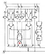
I attached the schematic of a DEM clock oscillator & attached shift-register that's probably used in the TDA1541A (Source, IEEE journal of solid state circuits, vol. SC-14, No. 3, June 1979).
The external DEM clock capacitor is marked in red. The outputs A, B, C, and D are the shift-register outputs for driving the electronic switches of the active current dividers. The outputs change in a certain pattern in order to average between the output currents of the passive divider that is part of the active divider. The end result is 4 closely matched output currents, derived from 4 passive output currents (passive current divider) that have certain tolerances and aren't fully matched.
When the DEM clock capacitor is removed, the DEM clock oscillator will run on stray capacitance (few pF), and produces a clock signal of around 7 MHz. By removing the capacitor and connecting these terminals to -V (-15V), using 2K2 resistors, oscillation stops. Now the external clock signal can be injected through 2 x 10 K Ohm, basically toggling the oscillator circuit with the external 352.8 KHz differential DEM clock that is derived from the low jitter master clock.
Without the 2K2 resistors, the DEM clock may produce unwanted spurious oscillations (short bursts of 7MHz clock signals), or may become unstable and stops. This is why DI4T performance kept varying. I plan to modify the D4T soon, and am very curious how this will affect performance.
TDA1543 doesn't require a DEM clock as it only contains passive current dividers, so this DEM clock "problem" doesn't occur with this chip.
so instead of building the differential 352khz DEM clock (derived from master clock) is it worth to try with only one 250 pF quality cap that will lock on 352.8 KHz on DEM pins (16,17)?
Is there big difference in sound using these two options compared to each other?
Tuning the capacitor is the easiest way for lowering DEM clock jitter amplitude, but jitter won't be as low as with an low jitter external DEM clock (DEM clock oscillator intrinsic jitter). So this modification improves sound quality over the 470 or 680pF, but still isn't optimal.
I attached the schematic of a DEM clock oscillator & attached shift-register that's probably used in the TDA1541A (Source, IEEE journal of solid state circuits, vol. SC-14, No. 3, June 1979).
The external DEM clock capacitor is marked in red. The outputs A, B, C, and D are the shift-register outputs for driving the electronic switches of the active current dividers. The outputs change in a certain pattern in order to average between the output currents of the passive divider that is part of the active divider. The end result is 4 closely matched output currents, derived from 4 passive output currents (passive current divider) that have certain tolerances and aren't fully matched.
When the DEM clock capacitor is removed, the DEM clock oscillator will run on stray capacitance (few pF), and produces a clock signal of around 7 MHz. By removing the capacitor and connecting these terminals to -V (-15V), using 2K2 resistors, oscillation stops. Now the external clock signal can be injected through 2 x 10 K Ohm, basically toggling the oscillator circuit with the external 352.8 KHz differential DEM clock that is derived from the low jitter master clock.
Without the 2K2 resistors, the DEM clock may produce unwanted spurious oscillations (short bursts of 7MHz clock signals), or may become unstable and stops. This is why DI4T performance kept varying. I plan to modify the D4T soon, and am very curious how this will affect performance.
TDA1543 doesn't require a DEM clock as it only contains passive current dividers, so this DEM clock "problem" doesn't occur with this chip.
Attachments
- Home
- Source & Line
- Digital Line Level
- Building the ultimate NOS DAC using TDA1541A