Ooops, you're right...
The new site lacks this info.
It is true it looks complicated for a novice but the DI16 isn't so...the detailed building instructions (PDF) make it an easy job. Believe me it is worth the pain.
8*4 update: I completed 7 heatsinks! I will try to mount the towers this weekend...
The new site lacks this info.
It is true it looks complicated for a novice but the DI16 isn't so...the detailed building instructions (PDF) make it an easy job. Believe me it is worth the pain.
8*4 update: I completed 7 heatsinks! I will try to mount the towers this weekend...
maxlorenz said:Ooops, you're right...
The new site lacks this info.
It is true it looks complicated for a novice but the DI16 isn't so...the detailed building instructions (PDF) make it an easy job. Believe me it is worth the pain.
8*4 update: I completed 7 heatsinks! I will try to mount the towers this weekend...
Yes, agree with that.
More i listening DI16 more i like it.
You have to test it. DI16 is sounding very realistic and natural.
I will try it also with low jitter module to get even better results. And 8x3 mod also...
I am very suprised, because these is not much entusiasm, about EC designs.
I begin really to respect, what John did and share.
John never ask me to write some post on forum at all!
I did that, because i wanted to share.
best regards, Bostjan
Hi langtuhanol,
The latest DI 8M version is best by a large margin now. It provides very high resolution, accurate phase, fast transient impulse response, and a holographic sound image.
DI 16 (8 * 3) is second, main reason is the approx. 10 times higher distortion of the TDA1543 chips when compared to the TDA1541A. It misses the sparkle and very high resolution of the DI 8M.
DI 16 is third, the DI 16 has fewer chips to average bit errors, so distortion is slightly higher. Due to the 16x interpolation, sound is slightly smoother.
You can find information about PCB-only kit pricing on my website, I will email detailed price list.
Main input: USB, with shiftregister reclocker (ultra low jitter 48 MHz master clock <1ps rms).
Optional input: DI2S (Differental I2S), external sources can be connected using the I2S signals. SPDIF sources can be connected trough external SPDIF > DI2S converter with shiftregister reclocker.
Main output is RCA, XLR is optional . Output voltage can be adjusted (resistors). I use 2V rms output signal amplitude for better signal to noise ratio.
This depends on interlink cable length and equipment used. Asymmetry in the connected (pre) amplifier can even result in higher distortion.
I now use rather extreme semi-balanced RCA interlinks (approx. 2.5mm wire diameter). They have 72 thin magnetically coupled lacquered copper wires for each conductor. Primary insulation is 3mm diameter PTFE (Teflon) tube. It has a copper braided screen. I use exactly the same wire construction for both signal and ground. The screen is connected to GND on one side only (the side with lowest impedance). I added a picture of these home-made interlinks.
They provide very high resolution / clarity, best tonal balance, and lowest noise levels so far.
Which is the better between DI8 and D16
The latest DI 8M version is best by a large margin now. It provides very high resolution, accurate phase, fast transient impulse response, and a holographic sound image.
DI 16 (8 * 3) is second, main reason is the approx. 10 times higher distortion of the TDA1543 chips when compared to the TDA1541A. It misses the sparkle and very high resolution of the DI 8M.
DI 16 is third, the DI 16 has fewer chips to average bit errors, so distortion is slightly higher. Due to the 16x interpolation, sound is slightly smoother.
I want to buy the better and how much is it?
You can find information about PCB-only kit pricing on my website, I will email detailed price list.
Input is RCA, USB, DI2S and XLR (balanced)?
Main input: USB, with shiftregister reclocker (ultra low jitter 48 MHz master clock <1ps rms).
Optional input: DI2S (Differental I2S), external sources can be connected using the I2S signals. SPDIF sources can be connected trough external SPDIF > DI2S converter with shiftregister reclocker.
Output is RCA, XLR (balanced)?
Main output is RCA, XLR is optional . Output voltage can be adjusted (resistors). I use 2V rms output signal amplitude for better signal to noise ratio.
I think XLR (balanced) is much better than RCA, isn't it?
This depends on interlink cable length and equipment used. Asymmetry in the connected (pre) amplifier can even result in higher distortion.
I now use rather extreme semi-balanced RCA interlinks (approx. 2.5mm wire diameter). They have 72 thin magnetically coupled lacquered copper wires for each conductor. Primary insulation is 3mm diameter PTFE (Teflon) tube. It has a copper braided screen. I use exactly the same wire construction for both signal and ground. The screen is connected to GND on one side only (the side with lowest impedance). I added a picture of these home-made interlinks.
They provide very high resolution / clarity, best tonal balance, and lowest noise levels so far.
Attachments
Hi -ecdesigns-,
Not trying to start a cable war, but we should all be thinking about what is written down here.
-Chris
Okay. You do know what you just said, right? Remember, these are copper wires.They have 72 thin magnetically coupled lacquered copper wires for each conductor.
Not trying to start a cable war, but we should all be thinking about what is written down here.
-Chris
Hi EC,
I will try this semi-balanced technique. Thanks.
The side with lowest impedance is always the "source", right?
You should really experiment with OCC copper magnet wire, if you can source it...
About my 8*4 DI-DAC, should I ground the heatsink/towers???
M
I now use rather extreme semi-balanced RCA interlinks (approx. 2.5mm wire diameter). They have 72 thin magnetically coupled lacquered copper wires for each conductor. Primary insulation is 3mm diameter PTFE (Teflon) tube. It has a copper braided screen. I use exactly the same wire construction for both signal and ground. The screen is connected to GND on one side only (the side with lowest impedance).
I will try this semi-balanced technique. Thanks.
The side with lowest impedance is always the "source", right?
You should really experiment with OCC copper magnet wire, if you can source it...
About my 8*4 DI-DAC, should I ground the heatsink/towers???
M


RCA interlinks
Hi anatech,
With magnetically coupled I mean that the stranded wires are twisted together (illustrated by photograph), similar to twisted pair network cable, perhaps I should have written electromagnetically coupled. My mistake.
The objective of this interlink construction is to achieve high resolution by reducing noise / losses.
I use a passive resistive volume control, so in this particular case, the (RCA) interlink quality becomes quite important. The gained advantage is eliminating pre-amplifier distortion.
Hi anatech,
Okay. You do know what you just said, right? Remember, these are copper wires.
With magnetically coupled I mean that the stranded wires are twisted together (illustrated by photograph), similar to twisted pair network cable, perhaps I should have written electromagnetically coupled. My mistake.
The objective of this interlink construction is to achieve high resolution by reducing noise / losses.
I use a passive resistive volume control, so in this particular case, the (RCA) interlink quality becomes quite important. The gained advantage is eliminating pre-amplifier distortion.
DI 8*3 / 8*4 heatsink construction
Hi maxlorenz,
In most cases the source has lowest impedance, the screen picks-up interference, it seems logical to dump these on the side with lowest impedance / lowest sensitivity.
About the copper wire type, there are more ways to provide a solution. One method is the use of special materials, another method is changing the construction.
Connect the heatsinks to chassis, put a 100nF capacitor between analog ground and chassis.
What matters most is functionality.
I added a photograph of my 8 * 3 heatsink construction, I use smaller aluminum blocks and a thin 2mm thick top plate in order to reduce heat accumulation. The top plate dissipates heat to the aluminum housing.
I hope you don't plan to solder the TDA1543 assemblies directly into the PCB. You need some play for compensating mechanical tolerances, and perhaps you need to remove some of the TDA1543 modules during testing.
About testing, one vital part is still missing.
Hi maxlorenz,
The side with lowest impedance is always the "source", right?
You should really experiment with OCC copper magnet wire, if you can source it...
In most cases the source has lowest impedance, the screen picks-up interference, it seems logical to dump these on the side with lowest impedance / lowest sensitivity.
About the copper wire type, there are more ways to provide a solution. One method is the use of special materials, another method is changing the construction.
About my 8*4 DI-DAC, should I ground the heatsink/towers???
Connect the heatsinks to chassis, put a 100nF capacitor between analog ground and chassis.
Not perfect but...who cares
What matters most is functionality.
I added a photograph of my 8 * 3 heatsink construction, I use smaller aluminum blocks and a thin 2mm thick top plate in order to reduce heat accumulation. The top plate dissipates heat to the aluminum housing.
Will try to test things tomorrow...
I hope you don't plan to solder the TDA1543 assemblies directly into the PCB. You need some play for compensating mechanical tolerances, and perhaps you need to remove some of the TDA1543 modules during testing.
About testing, one vital part is still missing.
Attachments
The SPDIF connection
Hi all,
Finally the SPDIF to (D)I2S interface with shiftregister reclocker is operational.
I added a photograph of the prototype.
This module connects SPDIF sources (CD / DVD player, satellite receiver) to DI 8M or DI 16. This way, a CDPROII can also be connected through the on-board SPDIF output.
The Crystal audio receiver converts the input signal to Philips format 64 BCK/WS. I used the CS8412 for now, The CS8414 can also be used (adapter socket).
It has the same shiftregister reclocker as the USBDI2S module. Provided the SPDIF source outputs the data correctly, sound quality should be identical to the USBDI2S module. SPDIF jitter is irrelevant, as long as the CS8412 / CS8414 PLL can get a good lock.
The master clock oscillator is the 48 MHz <1ps jitter clock. The crystal oscillator module has a SMD decoupling cap soldered directly to the power supply pads, and it's suspended over a small rubber sheet by means of 4 thin wires (to reduce the effect of external mechanical resonances).
The brand new 1:1 input transformer had an open circuit on the primary, so I had to make one myself.
Connections:
J1 (4-way), SPDIF in, 5V power supply.
J2 (5-way), I2S output (direct connection to the DI 8 or DI 16 core, also includes 5V power supply connection).
J3, (6-way), DI2S output (connection to the DI 8 / DI 16 external DI2S input).
If the direct I2S output is used (J2) both DS8921, and DS8922 chips (top right) aren't needed. PLL lock is indicated by a LED.
Attachments
Hi Sandor,
This transformer is just a temporary solution, as the new one I bought was defective. It's nothing special, took me only a few minutes to make, it's just a small ringcore (approx. 10mm diameter) with two windings of approx. 20 turns on it (wire diameter 0.2mm).
Can you, please, post details about your selfmade S/P-DIF input transformer?
This transformer is just a temporary solution, as the new one I bought was defective. It's nothing special, took me only a few minutes to make, it's just a small ringcore (approx. 10mm diameter) with two windings of approx. 20 turns on it (wire diameter 0.2mm).
Hi tubee,
As far as I have been able to test it, they sound exactly the same by direct comparison (toggling between USB and SPDIF). I used a fully modded DI 8M for testing. If there was even the slightest difference in sound quality, the DI 8M would reveal it.
This is good news as it shows that it's possible to achieve identical sound quality from two completely different digital sound sources (I used an old 500 MHz iMac for USB, and a very old Sony CD player with SPDIF coax output). The test CD was ripped and imported in iTunes, then placed in the Sony transport.
The tracks were started almost simultaneous, the sources were toggled by pulling the USB plug (this causes automatically switching to the SPDIF source). If there was a difference, this direct comparison of exactly the same tracks would show it.
Verification of BCK jitter showed the same clean very low jitter signal for both digital input sources. The BCK signal from the CS8412 (before reclocking) clearly showed jitter (approx. 250ps rms).
how is the sound of the spdif connection compared to the usb to I2S?
As far as I have been able to test it, they sound exactly the same by direct comparison (toggling between USB and SPDIF). I used a fully modded DI 8M for testing. If there was even the slightest difference in sound quality, the DI 8M would reveal it.
This is good news as it shows that it's possible to achieve identical sound quality from two completely different digital sound sources (I used an old 500 MHz iMac for USB, and a very old Sony CD player with SPDIF coax output). The test CD was ripped and imported in iTunes, then placed in the Sony transport.
The tracks were started almost simultaneous, the sources were toggled by pulling the USB plug (this causes automatically switching to the SPDIF source). If there was a difference, this direct comparison of exactly the same tracks would show it.
Verification of BCK jitter showed the same clean very low jitter signal for both digital input sources. The BCK signal from the CS8412 (before reclocking) clearly showed jitter (approx. 250ps rms).
Hi -ecdesigns-
Thanks for your tips (Post #1689)
As usual, very nice solution for your 8*3DAC.
My original plan was to place the main DI16PCB on the vertical axis to benefit from convective air cooling. I will try that if the horizontal position causes excessive heating. I think my construction is tight but will always fear accidental displacement of the towers and catastrophic short if horizontally placed.
I did not have cement/heat compound which would have helped to this problem and also to eventually put a folded heatsink on top of the present one. I will figure out a way to improve it if it is required.
Sorry, I did not get it. Would you explain?
Cheers,
M
Thanks for your tips (Post #1689)
As usual, very nice solution for your 8*3DAC.
My original plan was to place the main DI16PCB on the vertical axis to benefit from convective air cooling. I will try that if the horizontal position causes excessive heating. I think my construction is tight but will always fear accidental displacement of the towers and catastrophic short
if horizontally placed.I did not have cement/heat compound which would have helped to this problem and also to eventually put a folded heatsink on top of the present one. I will figure out a way to improve it if it is required.
About testing, one vital part is still missing.
Sorry, I did not get it. Would you explain?
Cheers,
M
Hi maxlorenz,
These heatsinks parts were CNC milled, but it was still quite difficult to assemble them. The heat dissipation works fine, the chips stay relatively cool and perform well. I already installed Arcol 0.1% resistors for I/V, diff amp and output attenuator. I still need to install the improved current source modules for pulling the LM4562 into class A.
I added a photograph of these new current source modules,
The IVDIF module on the left has the constant current source piggyback module installed. The module contains 3 precision current sources plus series resistor, and two decoupling capacitors (placed between +15V and -15V). I used low profile IC sockets to enable easy module removal.
The IVDIF module in the centre shows the gold-plated pins I soldered directly to the OP-amp sockets.
The piggyback module component side (bottom right), the current sources consist of 3 JFETs and two resistors. They provide approx. 3mA each.
The smaller single current source modules (top right) can be used for the DI 16, and tubediff input stage. I already experimented with a high voltage version for the cathode follower in the tubediff module, 4 JFETs, 2 resistors and a high-voltage power MOSFET. The result was even lower distortion in the tubedif amp.
You could use TO-220 silicone insulators and use them for both, heat transfer and insulation between heatsink and IC pins.
Thanks for your tips (Post #1689)
As usual, very nice solution for your 8*3DAC.
These heatsinks parts were CNC milled, but it was still quite difficult to assemble them. The heat dissipation works fine, the chips stay relatively cool and perform well. I already installed Arcol 0.1% resistors for I/V, diff amp and output attenuator. I still need to install the improved current source modules for pulling the LM4562 into class A.
I added a photograph of these new current source modules,
The IVDIF module on the left has the constant current source piggyback module installed. The module contains 3 precision current sources plus series resistor, and two decoupling capacitors (placed between +15V and -15V). I used low profile IC sockets to enable easy module removal.
The IVDIF module in the centre shows the gold-plated pins I soldered directly to the OP-amp sockets.
The piggyback module component side (bottom right), the current sources consist of 3 JFETs and two resistors. They provide approx. 3mA each.
The smaller single current source modules (top right) can be used for the DI 16, and tubediff input stage. I already experimented with a high voltage version for the cathode follower in the tubediff module, 4 JFETs, 2 resistors and a high-voltage power MOSFET. The result was even lower distortion in the tubedif amp.
I did not have cement/heat compound which would have helped to this problem and also to eventually put a folded heatsink on top of the present one. I will figure out a way to improve it if it is required.
You could use TO-220 silicone insulators and use them for both, heat transfer and insulation between heatsink and IC pins.
Attachments
Hi -ecdesigns-
You tell me!
(I sadly know how dificult is to put that together)
I asume you were talking about the current sources...I thought you were talking about my project...
Very nice little circuit for the lazy and ignorant amongst us
How about using silicone glue between IC pins and heatsinks? Will this degrade sound?
Regards,
M
These heatsinks parts were CNC milled, but it was still quite difficult to assemble them.
You tell me!
(I sadly know how dificult is to put that together)
About testing, one vital part is still missing.
I asume you were talking about the current sources...I thought you were talking about my project...
Very nice little circuit for the lazy and ignorant amongst us
How about using silicone glue between IC pins and heatsinks? Will this degrade sound?
Regards,
M
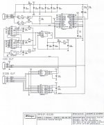
SPDIF > (D)I2S schematics
Hi anbello,
I added the schematic of the SPDIF to (D)I2S converter prototype.
CS8412 / CS8414 is put in the following mode:
Normal audio port mode (M3, pin17 = GND)
OUT, L/R, I2S Compatible. M0, pin23 = GND, M1, pin24 = VCC, M2, pin18 = GND)
Short explanation of schematic diagram:
SPDIF enters at J1 pin 3,4, and is fed to the CS8412 through a pulse transformer. A small ring core can be used for this, each winding should have approx. 225uH. L1 indicates PLL lock. CS8412/14 PLL jitter isn't critical.
Both SDATA, pin26 and FSYNC (WS) pin11 are available on J2 (I2S out), and converted to differential signals by U7 for the DI2S interface J3.
SCK (BCK) pin12 enters the shiftregister reclocker first (U2, U3, U4). The shiftregister reclocker is clocked by a very low jitter (<1ps) 48 MHz master clock (U5).
The reclocked BCK signal is available at U2, QB, pin4. It's then fed to the I2S interface, and converted to DI2S by U6.
I used a separate chip (U6) for BCK in order to reduce crosstalk. additional jitter problems can be caused by the DATA signal interfering (crosstalk) with BCK. I used miniature coax wire from Nexans for the I2S connections between modules.
Hi anbello,
Hi -ecdesigns-
i would like to see the schematics of the spdif receiver in Post #1690,
or at least to know in which mode is set the cs8412/14 (m0, m1, m2).
I added the schematic of the SPDIF to (D)I2S converter prototype.
CS8412 / CS8414 is put in the following mode:
Normal audio port mode (M3, pin17 = GND)
OUT, L/R, I2S Compatible. M0, pin23 = GND, M1, pin24 = VCC, M2, pin18 = GND)
Short explanation of schematic diagram:
SPDIF enters at J1 pin 3,4, and is fed to the CS8412 through a pulse transformer. A small ring core can be used for this, each winding should have approx. 225uH. L1 indicates PLL lock. CS8412/14 PLL jitter isn't critical.
Both SDATA, pin26 and FSYNC (WS) pin11 are available on J2 (I2S out), and converted to differential signals by U7 for the DI2S interface J3.
SCK (BCK) pin12 enters the shiftregister reclocker first (U2, U3, U4). The shiftregister reclocker is clocked by a very low jitter (<1ps) 48 MHz master clock (U5).
The reclocked BCK signal is available at U2, QB, pin4. It's then fed to the I2S interface, and converted to DI2S by U6.
I used a separate chip (U6) for BCK in order to reduce crosstalk. additional jitter problems can be caused by the DATA signal interfering (crosstalk) with BCK. I used miniature coax wire from Nexans for the I2S connections between modules.
Attachments
- Home
- Source & Line
- Digital Line Level
- Building the ultimate NOS DAC using TDA1541A