Hi arielpuri,
Thanks for your reply,
According to the people that already came over to listen to both DI DACs, the DI 8(M) sounds best, especially after the latest DEM clock mod. So I used the DI 8(M) as reference for the DI 16, and tried to match DI 16 sound quality to the DI 8M as closely as possible.
After some experimenting, it turned out that using 8 x interpolation for the DI 16 (8 x 3 TDA1543), resulted in a closer match with the DI 8M. So now the difference in sound quality is not so big anymore. Even the 8 x 2 configuration (using the same amount of DAC chips / similar THD), already resulted in a better match. So there are indications that 8x interpolation works better with a DI DAC. When using more TDA1543 chips in parallel, performance could be further improved, but after making some calculations, it would be quite problematic to obtain the same low distortion as with the TDA1541A, if possible at all.
The TDA1541A with it's 10 times lower distortion, used in a DI 8 configuration is quite difficult to beat. The calculated DAC chip THD of the DI 8 equals approx. 0.0006%, the DI 16 (8 x 3) equals approx. 0.0036%. THD is only one factor that determines DAC sound quality, but the lower distortion is a fact, and it is audible.
The audio equipment used must also perform at a high level in order to clearly hear all advantages of the DI 8M in full detail.
Thanks for your reply,
What sonic difference is now, between DI8 and DI16 DAC?
Is it big?
DI16 has 256x resolution, but DI8s TDA1541 has lower distortions.
That is not clear for me.
According to the people that already came over to listen to both DI DACs, the DI 8(M) sounds best, especially after the latest DEM clock mod. So I used the DI 8(M) as reference for the DI 16, and tried to match DI 16 sound quality to the DI 8M as closely as possible.
After some experimenting, it turned out that using 8 x interpolation for the DI 16 (8 x 3 TDA1543), resulted in a closer match with the DI 8M. So now the difference in sound quality is not so big anymore. Even the 8 x 2 configuration (using the same amount of DAC chips / similar THD), already resulted in a better match. So there are indications that 8x interpolation works better with a DI DAC. When using more TDA1543 chips in parallel, performance could be further improved, but after making some calculations, it would be quite problematic to obtain the same low distortion as with the TDA1541A, if possible at all.
The TDA1541A with it's 10 times lower distortion, used in a DI 8 configuration is quite difficult to beat. The calculated DAC chip THD of the DI 8 equals approx. 0.0006%, the DI 16 (8 x 3) equals approx. 0.0036%. THD is only one factor that determines DAC sound quality, but the lower distortion is a fact, and it is audible.
The audio equipment used must also perform at a high level in order to clearly hear all advantages of the DI 8M in full detail.
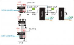
352.8 KHz DEM clock schematics
Hi all,
I mentioned the new 352.8 KHz DEM clock circuit a number of times now,
Here it is, I attached a diagram of the 352.8 KHz DEM clock I currently use.
Depending on BCK frequency, BCK needs to be divided by a specific factor in order to get 352.8 KHz. When BCK equals 2.8224 MHz, a divide by 8 counter is needed, with other BCK frequencies the division factor needs to be adapted.
2.1168 MHz > divide by 6
2.8224 MHz > divide by 8
4.2336 MHz > divide by 12
5.6448 MHz > divide by 16
11.2896 MHz > divide by 32
Division factors like 6 and 12 can be obtained by resetting the synchronous counter, depending on a specific counter output code. Division factors like 32 can be obtained by cascading synchronous counters. This is achieved by connecting the clock inputs (pin 2) together, and connecting the TC output of the first counter (pin 15) to both CEP (pin 7) and CET (pin 10) of the second one.
When using a synchronous counter with asynchronous reset like the 74HC161, a divide by twelve counter can be constructed by resetting the counter at output code 1100 (12). This will produce an asymetrical output signal. To correct this a divide by 6 counter can be constructed (reset code 0110), followed by a synchronous divide by 2 counter.
When using synchronous counters with synchronous reset like 74HC163, the same divide by 12 counter can be constructed by resetting the counter at output code 1011 (11) as the synchronous reset causes a 1 clock delay.
Resetting is done by using a NAND gate like the 74HC00 (dual input), 74HC10 (triple input) or 74HC20 (quad input) between outputs and the 74HC161 / 74HC163 reset (pin1). The "1" represented in the counter output code should be connected to the NAND gate inputs. So an output code of 1011 (11) would require 3 inputs (74HC10).
Don't use asynchronous ripple counters like the 74HCT4040, these will introduce unwanted delays that in turn cause inter modulations.
If multiple DAC chips are used, a common synchronous divider is used for all chips. Each chip needs a separate attenuator (680R / 180R), timing cap (470pF) connected to pin 16 and decoupling cap (100nF) connected to pin 17, this is also illustrated in the diagram
Attachments
Very interesting and useful circuit. I am a bit afraid, though, that there is some uncertainity of switching time (jitter) at the output of the 74HC161. I added a very simple reclocking right at the latch input of the TDA1541A. It is an old 74S74 high-speed D-type flip-flop. The original latch signal goes to its D input, and it is clocked from the master clock. Its Q output follows the D input precisely when the master clock next goes high. It reduces the jitter of the latch signal that might be produced by the previous circuitry. The same principle could be used after the DEM clock divider, utilizing the other half of the dual D-flip-flop. This also synchronizes the DEM clock positive edge with the DAC latch positive edge.
Re: 352.8 KHz DEM clock schematics
Quite frankly I tried both the old schematic at the beginning of this tread , and this last one .
Both exibit rather high distorsion at low levels playing music when applyed to the TDA1541A . Distorsion is data corruption alike .
The dac is with the CS8414 . Can it be so jittery to cause all of that , when without the DEM clock circuit it *seems* to work ok ?
Other people experienced that ? what about other DEM circuit reclocking used in combination with a spdif receiver ??
Thaaanks
-ecdesigns- said:Hi all,
I mentioned the new 352.8 KHz DEM clock circuit a number of times
Quite frankly I tried both the old schematic at the beginning of this tread , and this last one .
Both exibit rather high distorsion at low levels playing music when applyed to the TDA1541A . Distorsion is data corruption alike .
The dac is with the CS8414 . Can it be so jittery to cause all of that , when without the DEM clock circuit it *seems* to work ok ?
Other people experienced that ? what about other DEM circuit reclocking used in combination with a spdif receiver ??
Thaaanks
Re: Re: 352.8 KHz DEM clock schematics
I have heard artefacts in treble, once in a while. Used simple dem schematic with 161 or 163 divider to 176kHz, and no voltage divider, a coupling cap to pin 16 and pin 17 free floating. Replaced the 470pF cap later. Will try the new dem soon, have parts.
Btw (off topic): changed the 1N4007 diodes in HT PS from my hybrid power amp in BYV27-C's, sound is les coloured, cleaned up a lot. But have to get use to it, sometimes it's some "cold" and more remote. (analytic?)
Will try National HFA08TB60 8 amp. hexfreds in current section (powerfets) soon.
stefanobilliani said:
Quite frankly I tried both the old schematic at the beginning of this tread , and this last one .
Both exibit rather high distorsion at low levels playing music when applyed to the TDA1541A . Distorsion is data corruption alike .
The dac is with the CS8414 . Can it be so jittery to cause all of that , when without the DEM clock circuit it *seems* to work ok ?
Other people experienced that ? what about other DEM circuit reclocking used in combination with a spdif receiver ??
Thaaanks
I have heard artefacts in treble, once in a while. Used simple dem schematic with 161 or 163 divider to 176kHz, and no voltage divider, a coupling cap to pin 16 and pin 17 free floating. Replaced the 470pF cap later. Will try the new dem soon, have parts.
Btw (off topic): changed the 1N4007 diodes in HT PS from my hybrid power amp in BYV27-C's, sound is les coloured, cleaned up a lot. But have to get use to it, sometimes it's some "cold" and more remote. (analytic?)
Will try National HFA08TB60 8 amp. hexfreds in current section (powerfets) soon.
Re: Re: 352.8 KHz DEM clock schematics
Stefano,
where are you taking the "master" clock from? Maybe the BCK from CS8414 to TDA?
How does the waveform on pin 16 look like?
Cheers
Andrea
stefanobilliani said:
Quite frankly I tried both the old schematic at the beginning of this tread , and this last one .
Both exibit rather high distorsion at low levels playing music when applyed to the TDA1541A . Distorsion is data corruption alike .
The dac is with the CS8414 . Can it be so jittery to cause all of that , when without the DEM clock circuit it *seems* to work ok ?
Other people experienced that ? what about other DEM circuit reclocking used in combination with a spdif receiver ??
Thaaanks
Stefano,
where are you taking the "master" clock from? Maybe the BCK from CS8414 to TDA?
How does the waveform on pin 16 look like?
Cheers
Andrea
DEM clock
Hi stefanobilliani,
First of all you need to verify if the DEM clock circuit is functioning correctly. Conclusions are only valid with a correct working DEM clock.
I had similar problems with the first DEM clock I published last year, it didn't have the 100nF decoupling cap on pin 17. The attenuator must also be placed very close to pin 16, 17 and the GND connection, in order to avoid interference signals on the sensitive DEM clock oscillator input pins (pin 16 and 17).
The distortion you describe is that of a non-functional DEM clock (DEM clock is not able to drive the TDA1541A internal shift registers) so they stop, and low level distortion increases significantly as the Dynamic Element Matching system is no longer working. It is not caused by the CS8414.
I checked the DEM clock waveform on pin 16 with an oscilloscope, and removed a decoupling capacitor (MSB) to check the active divider output (20mV range), when the DEM clock functions correctly, a step shaped signal should be visible, it should have equal time for each step. The step pattern is caused by tolerances in the passive current divider (part of the active current divider).
I will try to post photograph showing both, DEM clock signal shape on pin 16, and the step signal on MSB (decoupling capacitor temporarily removed).
When both signals are correct, the DEM clock is working correctly, and low level signals should have very low distortion.
Hi stefanobilliani,
Quite frankly I tried both the old schematic at the beginning of this tread , and this last one .
Both exibit rather high distorsion at low levels playing music when applyed to the TDA1541A . Distorsion is data corruption alike .
The dac is with the CS8414 . Can it be so jittery to cause all of that , when without the DEM clock circuit it *seems* to work ok ?
First of all you need to verify if the DEM clock circuit is functioning correctly. Conclusions are only valid with a correct working DEM clock.
I had similar problems with the first DEM clock I published last year, it didn't have the 100nF decoupling cap on pin 17. The attenuator must also be placed very close to pin 16, 17 and the GND connection, in order to avoid interference signals on the sensitive DEM clock oscillator input pins (pin 16 and 17).
The distortion you describe is that of a non-functional DEM clock (DEM clock is not able to drive the TDA1541A internal shift registers) so they stop, and low level distortion increases significantly as the Dynamic Element Matching system is no longer working. It is not caused by the CS8414.
I checked the DEM clock waveform on pin 16 with an oscilloscope, and removed a decoupling capacitor (MSB) to check the active divider output (20mV range), when the DEM clock functions correctly, a step shaped signal should be visible, it should have equal time for each step. The step pattern is caused by tolerances in the passive current divider (part of the active current divider).
I will try to post photograph showing both, DEM clock signal shape on pin 16, and the step signal on MSB (decoupling capacitor temporarily removed).
When both signals are correct, the DEM clock is working correctly, and low level signals should have very low distortion.
Hi oshifis,
Thanks for your reply,
The external DEM clock circuit resulted in the biggest improvement of TDA1541A performance so far.
I already tested 74H..74 chips, they had the worst jitter specs from all D flip-flops I tested, so I don't use them anymore. Using 2 D flip-flops in the same housing for different frequencies causes crosstalk and should be avoided. Unused INPUTS should always be connected to a steady signal level (GND). I got lowest jitter using D flip-flops from 74HC164 and 74F164 shift registers, that's why I use them a lot for timing critical circuits. The lower jitter is probably caused by the chip internal circuit architecture.
The 74xx161 is a synchronous divider. This means that the outputs change state fully synchronous with the input clock signal (BCK). The 74HC161 triggers on the positive going edge of BCK, this means that 74HC161 outputs also change on the positive going edge of BCK. The jitter at the divider outputs is very low (comparable to 74HC164), reclocking it with a 74..74 would actually increase jitter.
Thanks for your reply,
Very interesting and useful circuit
The external DEM clock circuit resulted in the biggest improvement of TDA1541A performance so far.
I already tested 74H..74 chips, they had the worst jitter specs from all D flip-flops I tested, so I don't use them anymore. Using 2 D flip-flops in the same housing for different frequencies causes crosstalk and should be avoided. Unused INPUTS should always be connected to a steady signal level (GND). I got lowest jitter using D flip-flops from 74HC164 and 74F164 shift registers, that's why I use them a lot for timing critical circuits. The lower jitter is probably caused by the chip internal circuit architecture.
The 74xx161 is a synchronous divider. This means that the outputs change state fully synchronous with the input clock signal (BCK). The 74HC161 triggers on the positive going edge of BCK, this means that 74HC161 outputs also change on the positive going edge of BCK. The jitter at the divider outputs is very low (comparable to 74HC164), reclocking it with a 74..74 would actually increase jitter.
Re: DEM clock
The BCK is from the TDA1541A pin 2 , closely . Of course it comes from the CS8414 in this case .
Well the circuit is working ok . The cure was to put it very close to the pin 16-17 . Before I had it at 5 cm , while the BCK was connected at 1 cm distance , the output of the DEM reclock was too far . By very close I mean 1 cm or so.
Very nice improvement , now the distorsion at low levels is almost complitely gone . .... need to put the ear close to the speakers ( 96db 1W meter ) to detect some artifact .
Sorry no Scope yet ... but I wish ...")
Hello Andrea ,Andypairo said:
Stefano,
where are you taking the "master" clock from? Maybe the BCK from CS8414 to TDA?
Cheers
Andrea
The BCK is from the TDA1541A pin 2 , closely . Of course it comes from the CS8414 in this case .
Hello ecdesigns ,-ecdesigns- said:Hi stefanobilliani,
First of all you need to verify if the DEM clock circuit is functioning correctly. Conclusions are only valid with a correct working DEM clock.
I had similar problems with the first DEM clock I published last year, it didn't have the 100nF decoupling cap on pin 17. The attenuator must also be placed very close to pin 16, 17 and the GND connection, in order to avoid interference signals on the sensitive DEM clock oscillator input pins (pin 16 and 17).
I checked the DEM clock waveform on pin 16 with an oscilloscope, and removed a decoupling capacitor (MSB) to check the active divider output (20mV range), when the DEM clock functions correctly, a step shaped signal should be visible, it should have equal time for each step. The step pattern is caused by tolerances in the passive current divider (part of the active current divider).
Well the circuit is working ok . The cure was to put it very close to the pin 16-17 . Before I had it at 5 cm , while the BCK was connected at 1 cm distance , the output of the DEM reclock was too far . By very close I mean 1 cm or so.
Very nice improvement , now the distorsion at low levels is almost complitely gone . .... need to put the ear close to the speakers ( 96db 1W meter ) to detect some artifact .
Sorry no Scope yet ... but I wish ...
My Ecdesigns dem-clone is working too
Sounds good, its getting more to the core of the music, bass is deeper and clearer. Just putted it on, it has to warm up. I divided 11Mhz/16 (from dividerchip to 1541) and then with the suggested HCT161 /2, gives 350kHz.
Will see with scope how waveform looks.
Sounds good, its getting more to the core of the music, bass is deeper and clearer. Just putted it on, it has to warm up. I divided 11Mhz/16 (from dividerchip to 1541) and then with the suggested HCT161 /2, gives 350kHz.
Will see with scope how waveform looks.
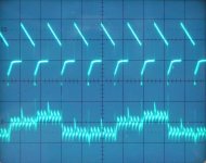
DEM clock and active divider output oscillogram
Hi tubee,
Thanks for your reply
Nice to hear you got better results now. I added an oscillogram I made today. Upper trace is the DEM clock (352.8 KHz), measured at pin 16. The sawtooth shaped ramp is generated by the 470pF timing cap and the DEM clock oscillator internal constant current source.
The lower trace is one of the 14 active divider outputs (100nF decoupling cap temporarily removed). It's clear to see that the step value changes synchronous with the DEM clock signal. This way correct DEM clock injection can be verified. Also visible is BCK crosstalk, this signal also shows that HF components need to be attenuated by the decoupling caps, so these caps should have low inductance.
We are looking at one (of the 4) outputs of the active current divider. Two passive current divider are closely matched on this particular output, the other two have tolerances.
One active divider output is switched sequentially between the 4 outputs of the preceding passive current divider. Since the output currents of these passive dividers have certain tolerances, it reflects in a unique step shaped ripple current at the active divider output. Every time the pattern is repeated, a full DEM clock cycle has been completed. It's clear to see it takes 4 DEM clock pulses to complete one full cycle.
The active divider is toggled on the negative going edge of the DEM clock.
By connecting a (100nF) decoupling cap to the active divider current output, the current ripple is averaged, resulting in a very accurate averaged DC current. The same happens with the other 4 active divider outputs. The idea is to get 4 exactly identical output currents, despite the tolerances in the passive divider. The TDA1541A has 3 of these active dividers (with each 4 outputs) for each channel. They correct the 6 MSBs.
The other 10 bits are generated by passive dividers, based on emitter scaling. They consist of 1024 darlington transistors.
The analog output signal is obtained by connecting combinations of the binary weighted currents to the DAC output by means of bit switches.
Hi tubee,
Thanks for your reply
My Ecdesigns dem-clone is working too
Sounds good, its getting more to the core of the music, bass is deeper and clearer. Just putted it on, it has to warm up. I divided 11Mhz/16 (from dividerchip to 1541) and then with the suggested HCT161 /2, gives 350kHz.
Will see with scope how waveform looks.
Nice to hear you got better results now. I added an oscillogram I made today. Upper trace is the DEM clock (352.8 KHz), measured at pin 16. The sawtooth shaped ramp is generated by the 470pF timing cap and the DEM clock oscillator internal constant current source.
The lower trace is one of the 14 active divider outputs (100nF decoupling cap temporarily removed). It's clear to see that the step value changes synchronous with the DEM clock signal. This way correct DEM clock injection can be verified. Also visible is BCK crosstalk, this signal also shows that HF components need to be attenuated by the decoupling caps, so these caps should have low inductance.
We are looking at one (of the 4) outputs of the active current divider. Two passive current divider are closely matched on this particular output, the other two have tolerances.
One active divider output is switched sequentially between the 4 outputs of the preceding passive current divider. Since the output currents of these passive dividers have certain tolerances, it reflects in a unique step shaped ripple current at the active divider output. Every time the pattern is repeated, a full DEM clock cycle has been completed. It's clear to see it takes 4 DEM clock pulses to complete one full cycle.
The active divider is toggled on the negative going edge of the DEM clock.
By connecting a (100nF) decoupling cap to the active divider current output, the current ripple is averaged, resulting in a very accurate averaged DC current. The same happens with the other 4 active divider outputs. The idea is to get 4 exactly identical output currents, despite the tolerances in the passive divider. The TDA1541A has 3 of these active dividers (with each 4 outputs) for each channel. They correct the 6 MSBs.
The other 10 bits are generated by passive dividers, based on emitter scaling. They consist of 1024 darlington transistors.
The analog output signal is obtained by connecting combinations of the binary weighted currents to the DAC output by means of bit switches.
Attachments
Re: DEM clock and active divider output oscillogram
Hi John.
I hear no artefacts now with this version, it seems music plays some slower now with it, i find that always a good sign. Soundstage is deeper.
Treble is still some sharp.(I have a new main speaker design in my head and should start building it. The planned tweeter could be much sweeter on the ear i suppose (B&G Neo 3) The now used Focal has a rising curve to 20k.)
Looked with scope at some waves: the 11Mhz masterclock (Kwak 7) it has not a squarewave anymore, but looks more like a sine, and is only 1,4V. When i fitted the clock it was square for sure. From the dividers they show allmost square and 2,5V.
scope on pin 16: Looks like a combination of your two traces: (sorry no dig. camera):
*The falling/rising edge is pinsharp now.
*The horizontal plateau is not really visible on scope here, but has a rising concave shaped curve. I hope it's not a problem.
*The sawtooth ramp has sharp spikes on them (with your upper dem trace it is a faint thicker line) and BCK remains are visible on the ramps (counted seven/ramp) I thought they where from the current divider caps, but indeed they are BCK remains because it is a divided frequency.
I removed the six pair 100N MKT's and one pair 0.47uF for MSB, replaced them by your advised value's. Took simple and cheap yellow MKT's 63V, no name, but shows an oblique "T" before value marking.
The 0.22uF's are blue MKT's (siemens?) like:
-ecdesigns- said:
Nice to hear you got better results now. I added an oscillogram I made today. Upper trace is the DEM clock (352.8 KHz), measured at pin 16. The sawtooth shaped ramp is generated by the 470pF timing cap and the DEM clock oscillator internal constant current source.
The lower trace is one of the 14 active divider outputs (100nF decoupling cap temporarily removed). It's clear to see that the step value changes synchronous with the DEM clock signal. This way correct DEM clock injection can be verified. Also visible is BCK crosstalk, this signal also shows that HF components need to be attenuated by the decoupling caps, so these caps should have low inductance.
Hi John.
I hear no artefacts now with this version, it seems music plays some slower now with it, i find that always a good sign. Soundstage is deeper.
Treble is still some sharp.(I have a new main speaker design in my head and should start building it. The planned tweeter could be much sweeter on the ear i suppose (B&G Neo 3) The now used Focal has a rising curve to 20k.)
Looked with scope at some waves: the 11Mhz masterclock (Kwak 7) it has not a squarewave anymore, but looks more like a sine, and is only 1,4V. When i fitted the clock it was square for sure. From the dividers they show allmost square and 2,5V.
scope on pin 16: Looks like a combination of your two traces: (sorry no dig. camera):
*The falling/rising edge is pinsharp now.
*The horizontal plateau is not really visible on scope here, but has a rising concave shaped curve. I hope it's not a problem.
*The sawtooth ramp has sharp spikes on them (with your upper dem trace it is a faint thicker line) and BCK remains are visible on the ramps (counted seven/ramp) I thought they where from the current divider caps, but indeed they are BCK remains because it is a divided frequency.
I removed the six pair 100N MKT's and one pair 0.47uF for MSB, replaced them by your advised value's. Took simple and cheap yellow MKT's 63V, no name, but shows an oblique "T" before value marking.
The 0.22uF's are blue MKT's (siemens?) like:
Attachments
I2S timing
Hello All ,
since this is the thread of the "timing" for excellence , why not fly a little off topic ( but not too much ) for a while .
I was interested and curious finding the information on this site RETRO AUDIO DAC (look at "the problem" section ) about the timing between the channels L and R of the audio samples .
Is someonelse aware of the fact that in the data stream the left sample arrive before the right sample ? And moreover is it a reliable information that on the " recording side" the 2 channels are made at the same time ?
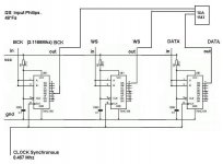
Well , I tried that on a 48*Fs system , with 3* 74HC164 and one TDA1543 per channel .
The results are interesting.....
One TDA1543 has the DATA shifted of 24 BCK and inverting its WS is just like shifting it of 24 BCK . So one TDA1543 works normally but has its outputs shifted ( delayed ) in the time domain.
The other TDA has the original DATA stram , but its WS is inverted ( delayed-shifted by 24 BCK )
So taking the audio output at both L pins of the TDA1543 offers the stereo set where the L sample is delayed of 24 BCK and the R sample is transferred to the DAC at the same time of its forerunner .
Does someone else tried this ? What are your impressions?Does it make sense for you?
Thanks for listening
Stefano
Hello All ,
since this is the thread of the "timing" for excellence , why not fly a little off topic ( but not too much ) for a while .
I was interested and curious finding the information on this site RETRO AUDIO DAC (look at "the problem" section ) about the timing between the channels L and R of the audio samples .
Is someonelse aware of the fact that in the data stream the left sample arrive before the right sample ? And moreover is it a reliable information that on the " recording side" the 2 channels are made at the same time ?
Well , I tried that on a 48*Fs system , with 3* 74HC164 and one TDA1543 per channel .
The results are interesting.....
One TDA1543 has the DATA shifted of 24 BCK and inverting its WS is just like shifting it of 24 BCK . So one TDA1543 works normally but has its outputs shifted ( delayed ) in the time domain.
The other TDA has the original DATA stram , but its WS is inverted ( delayed-shifted by 24 BCK )
So taking the audio output at both L pins of the TDA1543 offers the stereo set where the L sample is delayed of 24 BCK and the R sample is transferred to the DAC at the same time of its forerunner .
Does someone else tried this ? What are your impressions?Does it make sense for you?
Thanks for listening
Stefano
Sorry but I don't get it.
Being a serial bus some data has to come first and some after ;-)
The receiver (i.e. DAC) has some internal registers (memory) to store the word to be converted and then both conversions (L-R) should start at the same time, so it shouldn't matter at all which channel data comes first.
Or am I missing something?
Cheers
Andrea
Ciao Andrea , what about 2 mono dacs ??Andypairo said:Sorry but I don't get it.
Being a serial bus some data has to come first and some after ;-)
The receiver (i.e. DAC) has some internal registers (memory) to store the word to be converted and then both conversions (L-R) should start at the same time, so it shouldn't matter at all which channel data comes first.
Or am I missing something?
Cheers
Andrea
Ok inverting WS enable the dac to store the sample for the channel desired
In the listening things seems to be different anyway .
sometimes its all about experimenting
I know it sound absurd and nuts a little
inverting WS in a tda1543 has the effect of splitting the channels ( R go to L and L go to R ) but are they the same 2 samples in the time domain ? ( for what that may interest ? )
Andypairo said:Hi Stefano,
I'm afraid I don't have a answer for your question, maybe someone with more background on DACs
Cheers
Andrea
Thanks Andrea,its ok
L / R delays, DAC in mono / balanced mode
Hi stefanobilliani,
The RETRO DAC schematics show a AD1865 application that uses each DAC to construct a balanced output. DAC1 generates L + NL, DAC2 generates R + NR.
By using WS and NWS to latch the DAC chips, a delay between both L and R channels occurs. At NOS mode (44.1 KHz) this delay is half the period time or 1/44100/2 = 11.33 uS.
By delaying data for one channel, or by using so called clock stopping (freezing one channel clock input until the other channel has received all data), both L and R samples can be time-aligned again.
Since timing between both L and R channels is critical in obtaining correct spatial information, it makes sence to prevent delays between both channels.
First of all, the TDA1541A / TDA1543 latch the data automatically on the first positive going edge of BCK after WS has gone low. Internal registers / latches are used to ensure that both samples occur at the DAC output simultaneously.
Your circuit is similar to taking the left signal from the left output of DAC nr. 1 and the right channel from the right output of DAC nr. 2. Your example might have the advantage that the same circuits are used on each DAC chip (only the left channel).
About your example:
TDA1541A nr. 1, delay 24BCK inverting WS, L output = L-1, R output = R-1
TDA1541A nr. 2, inverting WS, L output = R-1, R output = L
Now when taking stereo information from both L channels it results in
L output TDA1541A nr. 1 = L-1
L output TDA1541A nr. 2 = R-1
BCK would become problematic, DAC nr. 1 would receive delayed data that changes on the positive going edge of BCK (otherwise the data couldn't be sampled by the shiftregister). DAC nr. 1 needs to receive NBCK in order to sample correctly
DAC chip nr. 2 would receive normal data, so it needs BCK.
So the correct L + R data is output, and is time aligned (because both WS signals are inverted), but they do have a small time delay of 1/BCK/2.
Since both chips process / generate L + R channels as indicated, crosstalk between both channels is still present in both TDA1541A chips so the circuit isn't optimal.
It's better to change the circuit so one chip would receive L + NL or L + L, and the other receives R + NR or R + R. This way crosstalk could be reduced, and output current is doubled.
Hi stefanobilliani,
I was interested and curious finding the information on this site RETRO AUDIO DAC (look at "the problem" section ) about the timing between the channels L and R of the audio samples .
The RETRO DAC schematics show a AD1865 application that uses each DAC to construct a balanced output. DAC1 generates L + NL, DAC2 generates R + NR.
By using WS and NWS to latch the DAC chips, a delay between both L and R channels occurs. At NOS mode (44.1 KHz) this delay is half the period time or 1/44100/2 = 11.33 uS.
By delaying data for one channel, or by using so called clock stopping (freezing one channel clock input until the other channel has received all data), both L and R samples can be time-aligned again.
Since timing between both L and R channels is critical in obtaining correct spatial information, it makes sence to prevent delays between both channels.
Well , I tried that on a 48*Fs system , with 3* 74HC164 and one TDA1543 per channel .
The results are interesting.....
One TDA1543 has the DATA shifted of 24 BCK and inverting its WS is just like shifting it of 24 BCK . So one TDA1543 works normally but has its outputs shifted ( delayed ) in the time domain.
The other TDA has the original DATA stram , but its WS is inverted ( delayed-shifted by 24 BCK )
So taking the audio output at both L pins of the TDA1543 offers the stereo set where the L sample is delayed of 24 BCK and the R sample is transferred to the DAC at the same time of its forerunner .
Does someone else tried this ? What are your impressions?Does it make sense for you?
First of all, the TDA1541A / TDA1543 latch the data automatically on the first positive going edge of BCK after WS has gone low. Internal registers / latches are used to ensure that both samples occur at the DAC output simultaneously.
Your circuit is similar to taking the left signal from the left output of DAC nr. 1 and the right channel from the right output of DAC nr. 2. Your example might have the advantage that the same circuits are used on each DAC chip (only the left channel).
About your example:
TDA1541A nr. 1, delay 24BCK inverting WS, L output = L-1, R output = R-1
TDA1541A nr. 2, inverting WS, L output = R-1, R output = L
Now when taking stereo information from both L channels it results in
L output TDA1541A nr. 1 = L-1
L output TDA1541A nr. 2 = R-1
BCK would become problematic, DAC nr. 1 would receive delayed data that changes on the positive going edge of BCK (otherwise the data couldn't be sampled by the shiftregister). DAC nr. 1 needs to receive NBCK in order to sample correctly
DAC chip nr. 2 would receive normal data, so it needs BCK.
So the correct L + R data is output, and is time aligned (because both WS signals are inverted), but they do have a small time delay of 1/BCK/2.
Since both chips process / generate L + R channels as indicated, crosstalk between both channels is still present in both TDA1541A chips so the circuit isn't optimal.
It's better to change the circuit so one chip would receive L + NL or L + L, and the other receives R + NR or R + R. This way crosstalk could be reduced, and output current is doubled.
Re: L / R delays, DAC in mono / balanced mode
Many thanks ecdesigns for your reply .
Well in my tests I forget to invert BCK for the shifted channel , infact that is why the difference in the stereo imagine was so big and the channel wanst reproduced correctly .
If you are able to produce a schematic for 48Fs system that ebable one TDA to rerpoduce L and - L ( or L+L ) and the other R and -R( or R+R ) I would be grateful .
Thanks
-ecdesigns- said:Hi stefanobilliani,
The RETRO DAC schematics show a AD1865 application that uses each DAC to construct a balanced output. DAC1 generates L + NL, DAC2 generates R + NR.
By using WS and NWS to latch the DAC chips, a delay between both L and R channels occurs. At NOS mode (44.1 KHz) this delay is half the period time or 1/44100/2 = 11.33 uS.
By delaying data for one channel, or by using so called clock stopping (freezing one channel clock input until the other channel has received all data), both L and R samples can be time-aligned again.
Since timing between both L and R channels is critical in obtaining correct spatial information, it makes sence to prevent delays between both channels.
First of all, the TDA1541A / TDA1543 latch the data automatically on the first positive going edge of BCK after WS has gone low. Internal registers / latches are used to ensure that both samples occur at the DAC output simultaneously.
Your circuit is similar to taking the left signal from the left output of DAC nr. 1 and the right channel from the right output of DAC nr. 2. Your example might have the advantage that the same circuits are used on each DAC chip (only the left channel).
About your example:
TDA1541A nr. 1, delay 24BCK inverting WS, L output = L-1, R output = R-1
TDA1541A nr. 2, inverting WS, L output = R-1, R output = L
Now when taking stereo information from both L channels it results in
L output TDA1541A nr. 1 = L-1
L output TDA1541A nr. 2 = R-1
BCK would become problematic, DAC nr. 1 would receive delayed data that changes on the positive going edge of BCK (otherwise the data couldn't be sampled by the shiftregister). DAC nr. 1 needs to receive NBCK in order to sample correctly
DAC chip nr. 2 would receive normal data, so it needs BCK.
So the correct L + R data is output, and is time aligned (because both WS signals are inverted), but they do have a small time delay of 1/BCK/2.
Since both chips process / generate L + R channels as indicated, crosstalk between both channels is still present in both TDA1541A chips so the circuit isn't optimal.
It's better to change the circuit so one chip would receive L + NL or L + L, and the other receives R + NR or R + R. This way crosstalk could be reduced, and output current is doubled.
Many thanks ecdesigns for your reply .
Well in my tests I forget to invert BCK for the shifted channel , infact that is why the difference in the stereo imagine was so big and the channel wanst reproduced correctly .
If you are able to produce a schematic for 48Fs system that ebable one TDA to rerpoduce L and - L ( or L+L ) and the other R and -R( or R+R ) I would be grateful .
Thanks
- Home
- Source & Line
- Digital Line Level
- Building the ultimate NOS DAC using TDA1541A