Hi tubee,
Thanks for your reply [post #1394]
Resistor ladder DAC chips like the PCM56 use a voltage reference source that feeds a resistor ladder network. The output impedance of the ladder network is not constant, and varies with the bit switch settings. When a passive I/V resistor is connected to it, this will lead to audible bit errors. The PCM56 can only function correctly if it feeds into virtual ground (OP-amp). With TDA1541A / TDA1543 it's similar, violating the maximum allowable output compliance of 25mV produces higher bit errors than specified in the datasheet.
So I personally don't use passive I/V converters because I try to get lowest possible bit errors.
I use highly optimized the OP-amp I/V stages now, this includes external biasing (cascode). External biasing is not the same as increasing the (OP-amp) internal bias current. For I/V converters it's important to use fast OP-amps, operate them in the output voltage range where they produce lowest distortion, and keeping capacitive loads as low as possible.
If you accept bit errors by using passive I/V, and also add a tube output stage, some new problems occur:
- Tubes produce relatively high noise levels,
- The anode / filament supply can easily introduce hum
- Tubes have relatively high output impedance
- A coupling capacitor is often needed, causing sound coloration
The "sound" of a DAC chip relies heavily on the circuit it's used in. In order to achieve optimal results, extensive tuning is necessary.
DAC chips like the TDA1541A were probably never used optimally, because I didn't see a correct working DEM clock circuit yet. Using the TDA1541A internal DEM clock causes huge jitter, this can be easily measured (PIN 16 & 17). Jitter on the DEM clock causes incorrect active divider operation (divided currents are no longer accurately averaged / matched). Without a perfect working DEM clock, the TDA1541A produces fluctuating bit errors (bit errors vary with the DEM clock duty-cycle variations. The effect on sound quality is similar to jitter on the timing signal (BCK).
The TDA1541A-S2 is selected for lowest bit errors, probably the standard DEM clock was used during this selection process (so DEM clock wasn't optimal). A possible way to still achieve low bit errors with a bad DEM clock is that the active dividers already have very high initial accuracy.
Another problem is that DEM clock interference finds it's way to the TDA1541A output (crosstalk), when using a free running DEM clock, this will introduce intermodulation distortion. Therefore it's important to synchronize the DEM clock with BCK. In order to complete a full DEM cycle (DEM switch matrix has 4 switch settings) within one sample, optimal DEM clock (with a NOS DAC) equals 44100 * 4 = 176.4 KHz (DEM clock frequency is specified between approx. 150...250 KHz).
With oversampling (4X) this means that there isn't enough time to complete a full DEM cycle before the next sample has to be output. So bit errors / fluctuations might be slightly higher now.
I have tried to find the reason for the natural sound quality of NOS DACs. By experimenting with band-limiting (brickwall filtering) signals from tape decks and record players, it seems like the band-limiting itself already produces a synthetic, unnatural sound. Further experiments show that a NOS DAC (because it's not band-limited like a OS DAC) is capable of producing faster signal transients (similar like with the tape deck and record player that are also not band-limited to 20 KHz). This might well be one of the reasons why NOS DACs produce a sound that appears to be more natural.
Next "problem" with digital filters is that they replace the original samples with calculated ones. Each sample leaving a digital interpolation filter is a result of a averaging / calculation process using 100+ samples. So the outcome of this calculation process is entirely responsible for the sound quality. The slightest trunctuations can completely change the sound spectrum. Basically, when listening to a OS DAC, one is listening to the results of calculations, not the original samples.
An example, suppose we average between 100 samples and 5 of them have a slightly different value (few bit difference), it's very likely that these relatively small fluctuations are completely "filtered" out by averaging / trunctuation process. So basically, micro-information present in the original samples could be simply removed this way.
A NOS DAC will re-produce this micro-information, but it's likely to disappear below the noise level caused by quantization noise (16 bit 44.1 KHz), as the (time) resolution is rather low.
The DI DACs change this, by significantly increasing both time, and analog resolution, quantisizing error amplitude will drop significantly. Now all micro-information is lifted above the noise floor and becomes clearly audible. Because the DI DACs only interpolate between few samples, and amplitude "calculations" are performed by a analog circuit (multiple DAC chips), no trunctuation errors occur. In fact this system even increases bit resolution by providing additional analog values.
The DI DAC analog output signal now has both, Higher amplitude resolution (19 or 20 bits) and higher time resolution (8 or 16 times higher). So a DI 8(M) ends up with approx. 64x resolution enhancement, the DI 16 with 256x resolution enhancement.
By comparison the 4x oversampled signal from a SAA7220 / TDA1541A combination only provides 4x resolution enhancement!
Another problem with OS DACs is that they shift the mirror images up the frequency spectrum (with a NOS DAC they are located relatively close to the audio range). By doing so, the HF signal / HF energy has to pass both, the analog part of the D/A converter AND the I/V stage / analog output stage, before it enters the analog corrective filter. Any non-linearity will now introduce errors. This might also be the reason for the OS DAC high jitter sensitivity (frequency modulated HF images).
The DI DACs interpolate as well, they also produce higher virtual sample rates, but each DAC chip still runs in NOS mode, the mirror images at higher frequencies have less power now (each image has less power than the fundamental image). The jitter sensitivity of a DI 8M is much lower than a OS DAC with 8x oversampling, this seems to indicate that the jitter "problem" is not merely caused by slight sample timing errors, but rather by analog circuit disruption, caused by the frequency modulated HF images. The FM HF images introduce problems with non-linear components / circuits.
OS DACs have pre-ringing, this almost never occurs with real-life sounds, so we might perceive it as unnatural sounding. It could also limit dynamics.
DI DACs have zero pre- and post ringing. The impulse response is totally flat. Dynamics are optimal.
Hi -ecdesigns--ecdesigns- said:DAC chips like the TDA1541A were probably never used optimally, because I didn't see a correct working DEM clock circuit yet. Using the TDA1541A internal DEM clock causes huge jitter, this can be easily measured (PIN 16 & 17). Jitter on the DEM clock causes incorrect active divider operation (divided currents are no longer accurately averaged / matched). Without a perfect working DEM clock, the TDA1541A produces fluctuating bit errors (bit errors vary with the DEM clock duty-cycle variations. The effect on sound quality is similar to jitter on the timing signal (BCK).
I intend to use an external 176.4 kHz clock here, divided from the low-jitter master clock. Which pin should I use for the input, pin 16 or pin 17, and do I need the other pin left open? Can I use TTL level signal?
BTW, if you spent so much effort in the digital part, you should try my transformer/tube I/V circuit. It sounds much better than the OPA627 that I used before.
http://www.diyaudio.com/forums/showthread.php?s=&threadid=100297
Regards,
Laszlo
Hi John
Thanks for explaining of your TDA choice and tips for PCM experiments. Will read it over thourough.
My first comment now is: I first did dem in the simple way: divided with 74/163 to 176Khz, no extra components, only a coupling cap to pin 16. Now i removed Dem reclock, replaced a 470pF Philips KP cap between 16-17, because i sometimes heard artefacts in treble. I should use your transformer coupled dem schematic with bead filtering.
The sound without dem divider: a little warmer (more jitter?) and maybe a slightly more diffuse stereo image, that's all. But the artefacts are gone.
"
- Tubes produce relatively high noise levels,
- The anode / filament supply can easily introduce hum
- Tubes have relatively high output impedance
- A coupling capacitor is often needed, causing sound coloration "
I made a regulated PS for f-f
Have some Ropel 3.3 uF MKP caps.
Output impedance is not important to me, the stage has to drive a 50cm cable to tubed pre-amp.
Only the noise can be some concearn.
-ecdesigns- said:
Resistor ladder DAC chips like the PCM56 use a voltage reference source that feeds a resistor ladder network. The output impedance of the ladder network is not constant, and varies with the bit switch settings. When a passive I/V resistor is connected to it, this will lead to audible bit errors. The PCM56 can only function correctly if it feeds into virtual ground (OP-amp).
I can't agree with that.
With the PCM56, the passive I/V works very good up to > 500 ohms.
Bernhard said:
I can't agree with that.
With the PCM56, the passive I/V works very good up to > 500 ohms.
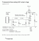
I guess the lower the I/V resistor, the lower the distorsion. but lower output voltages has to be amplified more, it's a matter of the right choices. Triodedick advises 100 ohm for I/V res.
(btw i don't know where the zobel is for)
Attachments
Re: Re: Re: Re: DAC chips
Almost two years, at that time I selected chips, so should be good ones.
Did they have any stickers/labels ?
tubee said:
Don't know what selection criteria you handled at that time Bernard. I purchased them together with a CD304, remember? (june 2005??)
Almost two years, at that time I selected chips, so should be good ones.
Did they have any stickers/labels ?
tda541a where to buy
Hello,
For those looking for a tda1541a source check the following site:
http://www.diyparadiso.com/
got the sales or "uitverkoop" part, tda1541a 10 euro each.
Keep on building
Hello,
For those looking for a tda1541a source check the following site:
http://www.diyparadiso.com/
got the sales or "uitverkoop" part, tda1541a 10 euro each.
Keep on building
Hi oshifis,
Thanks for your reply [post 1402]
You need to use a synchronous divider like the 74HCT161, if you need a higer division factor, multiple 74HCT161 chips can be cascaded (examples can be found in the datasheet).
Now make a voltage divider by connecting 2 x 100 Ohm resistor in series between 176.4 KHz output and AGND, creating a 2.5Vpp signal. Now connect a 100pF capacitor between the 2.5Vpp tap and pin 16 of the TDA1541A. Use a high quality polypropylene (WIMA) or polystyrene capacitor (LCR components).
Connect a 100nF film bypass capacitor (WIMA or BC components) between pin 17 and AGND.
The upper oscillogram shows the typical "datasheet" DEM clock, needless to say it contains jitter.
The lower oscillogram shows the synchronized low jitter DEM clock. This is how the output signal on pin 16 should look like (you may need to experiment with both signal amplitude (2.5V) and capacitor value (100pF).
No offense but I already have a hybrid output stage (tube OP-amp plus semiconductor Op-amp in parallel). I am convinced that it's able to outperform both a semiconductor-only or tube-only output stage. It has new sonic properties, unlike typical tube or semiconductor circuits.
I feed both tube Op-amp and semiconductor OP-amp with a OP-amp I/V converter, so I fully meet TDA1541A output compliance, achieving very low non-linear distortion.
I avoid using transformers and capacitors whenever possible, they are non-linear devices that can easily colour / smear the sound. I use DC coupled circuits whenever possible.
I no longer use the OPA627, I can imagine that a good tube output stage could outperform it. The OPA627 sound darks / laid-back, and veiled. It can't achieve the LM4562 transparency, even when forced into class A.
I now use the LM4562 "sweet spot" for lowest THD, and added a external tuning circuit that significantly reduces crossover distortion, and stabilizes the negative feedback loop. I also kept capacitive load very low (settling time). Used this way, the LM4562 is hard to beat.
Don't forget, my aim is not to achieve a nice sounding DAC.
My aim is to achieve very realistic "live" performance from my audio set. I use sonic resonators (point source) to achieve this. These have a special mechanism to re-construct a 3D sound image, using only 2 channels.
This requires staggering performance from both DAC and power amplifier, and makes DAC design much more difficult. Playing both high-quality live recordings and Chesky audio recordings, it seems I almost reached that aim.
It's not possible to obtain this effect with (bad) studio recordings, it only works with good live recordings that are not tampered with too much.
This more or less proves that the system works.
Attachments

Hi tubee,
Thanks for your reply [post #1403]
I explained the new DEM circuit in post #1402
I had to remove the DEM clock filtering again, it introduced significant jitter. The jitter is much worse than the slight HF interference.
About tube noise and hum. You could design a clever circuit that counter-acts the hum on both anode voltage and filament, but it's critical. I also used a regulated DC voltage for the filaments, I connected one side of the filament to ground. Leaving the filaments floating, causes hum and noise.
I used a stabilized anode voltage and capacitance multiplier for each anode, hum is now completely gone. Note that a single zener reference is not accurate enough, I used 2 cascaded zeners to drive the capacitance multipliers. The first one provides a very stable supply voltage for the second one. The second one will then provide exceptional stability.
By paralleling both tube OP-amp and semiconductor OP-amp, using a specific "mixing ratio", the tube noise is significantly reduced.
Re: Re: Re: Re: Re: DAC chips
Hi Bernard.
They had no labels. But one had a blue marker stripe over it, the other red. They are selected allright for sure, they sound both exact the same when swapped.
With the zobel of the Triodedick scheme i mean the 22R/22N in series after dac output. I assume it's a @44.1Khz tuned extra filter.
Bernhard said:
Almost two years, at that time I selected chips, so should be good ones.
Did they have any stickers/labels ?
Hi Bernard.
They had no labels. But one had a blue marker stripe over it, the other red. They are selected allright for sure, they sound both exact the same when swapped.
With the zobel of the Triodedick scheme i mean the 22R/22N in series after dac output. I assume it's a @44.1Khz tuned extra filter.
-ecdesigns- said:Hi tubee,
Thanks for your reply [post #1403]
I explained the new DEM circuit in post #1402
I had to remove the DEM clock filtering again, it introduced significant jitter. The jitter is much worse than the slight HF interference.
Thanks again John for useful tips.
When i see you perfect dem signals on scope, i see your thourough work. I see now i missed that you altered the dem schematic. My simple dem schematic was wrong too. Will try your new schem. on CD304mk2 sometime. And have about six tda1541's left for further experiments... should still finish my 4 tda dac.... if i had time..
For HT regulator i am using a series regulator with a 5A fet, IRF830 or something. I like the use of chokes in ps too, even a simple tubelight choke will do fine in a HT supply.
I could not manage to hook f-f on Gnd, a smoking resistor was the result.

Hi EC,
DI16core PCB arrived yesterday")
The iron is HOT today...and so am I
One doubt aroused:
On the I2S connection holes, first one says "VCC". I got lost here.
I thought (and still think, looking at the traces) that the timing chain get its power from the regulator...
Can you enlight me?
BTW, the PCB looks gorgeous!
(I hate that english word but I have to admit that it fits the situation here).
Thanks,
M
DI16core PCB arrived yesterday
The iron is HOT today...and so am I
One doubt aroused:
On the I2S connection holes, first one says "VCC". I got lost here.
I thought (and still think, looking at the traces) that the timing chain get its power from the regulator...
Can you enlight me?
BTW, the PCB looks gorgeous!
(I hate that english word but I have to admit that it fits the situation here).
Thanks,
M
Hi maxlorenz,
Good to hear the PCB arrived,
About VCC on the I2S connector, this is an output. It's used to feed the DI2S receiver / switch, on the USB/DI2S module. It can also be used to feed external circuits.
All circuits on the DI 16 core (timing-chain inclusive) receive their power supply from on-board voltage regulators.
OP-amps(U33...U35): +15V regulator (U39) and -15V regulator (U40)
DAC group 1 (U17...U24): +6V regulator (U36)
DAC group 2 (U25...U32): +6V regulator (U37)
Timing-chain, clock buffers / external circuits, +5V regulator (U38)
The iron was burning hot today and I am done soldering the PCBs. All sockets and components are placed
Ufortunately... I am too tired to continue tonight and am leaving on saturday to go to india for business & czech republic to visit some family.
I can't wait to test everything, socket the chips, create the cables and sit back and listen
probably going to be a couple of weeks till I get to it though.
..David
Hi EC,
Oh! I see...
And jumper "JP1" must be linked (R17 to VCC) for normal operation, right?
(I forgot that part...)
Another Q:
IF I need more Vout, can I invert the order of the resistors at the V divider? (R13/R15, if I remember well...)
Cheers,
M
About VCC on the I2S connector, this is an output. It's used to feed the DI2S receiver / switch, on the USB/DI2S module. It can also be used to feed external circuits.
Oh! I see...
And jumper "JP1" must be linked (R17 to VCC) for normal operation, right?
(I forgot that part...)
Another Q:
IF I need more Vout, can I invert the order of the resistors at the V divider? (R13/R15, if I remember well...)
Cheers,
M
Hi David,
I'm so sorry to hear... 
I want mine to be SN 000000001
On another thought, why don't you put the kit and all the parts on your lugage...that's what i would do I'm sure your family will understand
Good luck!
M
Unfortunately... I am too tired to continue tonight and am leaving on saturday to go to india for business & czech republic to visit some family.
I'm so sorry to hear...
I want mine to be SN 000000001
On another thought, why don't you put the kit and all the parts on your lugage...that's what i would do
I'm sure your family will understand Good luck!
M
I asked John a few questions over the last couple of weeks and he's been super helpful.
I thought it would be helpful if I posted a couple of these here, since I see others now working on their PCBs.
I'm using Di16core without the tube stage.
1st question was about adding balanced outputs in addition to the RCA outs,
J3
DI16C, J3 PIN1=LEFT OUT, connected to center tap RCA (screened
cable), white
DI16C, J3 PIN2=LEFT GND, connected to GND RCA (screen)
DI16C, J3 PIN3 = not connected
DI16C, J3 PIN4 = not connected
DI16C, J3 PIN5 = not connected
DI16C, J3 PIN6 = not connected
DI16C, J3 PIN7 = not connected
DI16C, J3 PIN8 = not connected
DI16C, J3 PIN9=RIGHT GND, connected to GND RCA (screen)
DI16C, J3 PIN10=RIGHT OUT, connected to center tap RCA (screened
cable), red
John said use both the IV and NIV outputs of each channel (J3 pin 3+4 and 7+8). These provide both the inverted and non-inverted output for each channel.
NIV(L) -- 2K --> Nout(L) -->500R --> GND. Nout(L) is the inverted left output voltage at the 2k / 500R junction
IV(L) -- 2K --> out(L) -->500R --> GND. out(L) is the non-inverted left output voltage at the 2K / 500R junction
NIV(R) -- 2K -- Nout(R) --> 500R --> GND. Nout(R) is the inverted right output voltage at the 2K / 500R junction
IV(R) -- 2K --> our(R) --> 500R --> GND. out(R) is the non-inverted right output voltage at the 2K / 500R junction
GND goes to the GND terminal on the XLR connectors.
2nd question I asked John was about assembly instructions on DI16core that had 510ohm output in assembly instructions for R15/16. (i noticed John had 1k in his parts list).
I asked him about this and he said this resistor determines DI 16 output voltage, he uses 2V rms in his system (R15, R16 =1 K Ohm) for optimal S/N ratio, however, 1V rms is the standard and requires the 510 Ohm resistor value. So this value
depends on the output voltage you require.
I looked up spec on my amp and noticed it needs 1.125v to run at full power suo I upped this slightly to 562R.
Hi maxlorenz,
Thanks for your reply [post #1417]
Jumper JP1 is for selecting single-ended or differential mode of the timing-chain.
Differential mode (default) inverts the data of one DAC group (8 data lines in total):
> JP1 left OPEN.
> U13 = 74HC(T)00, NAND gates.
Single-ended mode (for experimenting) does not invert data of DAC groups:
> JP1 CLOSED.
> U13 = 74HC(T)08, AND gates.
Four data bits are toggled by the PAL (Programmable Array Logic), a chip that can be programmed to perform specific digital functions.
The other 4 databits are "toggled" by using either a inverting, or a non inverting gate with the same pin lay-out.
DI 16 output voltage:
The DI DACs have 3 analog outputs for each channel:
NIV > inverting I/V converter output ( can be used to drive a balanced stage / XLR).
IV > non-inverting I/V converter output ( can be used to drive a balanced stage / XLR).
OUTPUT > single ended output (RCA).
The output voltage amplitude depends on:
> I/V resistors (R1...R4), generated voltage is roughly 0.016 * I/V resistor value. This voltage appears at NIV and I/V outputs.
example: 470R will produce approx. 0.016 * 470 = 7.52 Vpp.
The diff amp has unity gain and adds the voltages from both I/V stages, with 470 Ohm I/V resistors, output voltage is now approx. 7.52 * 2 = 15.04 Vpp.
> Output attenuator (R13, R15 and R14, R16).
I used 2 K ohm of series resistance for the DI 16, but this value can be lowered to approx. 600 Ohms. This will provide lower output impedance.
I used separate pins (from a turned-pin IC socket) for mounting these resistors. This way you they can be easily swapped for experimenting. Same applies for the I/V resistors.
Suppose you want an output voltage of 7 Vpp and a 1 K Ohm total series resistance:
Attenuation factor needed is 7 / 15.4 = 0.45
R15, R16 = 1000 * 0.45 = 450 Ohms
R13, R14 = 1000 - 450 = 550 Ohms.
- Home
- Source & Line
- Digital Line Level
- Building the ultimate NOS DAC using TDA1541A