SoNic_real_one said:
So, if I got it right, in the case of using 8 DAC's, for the first 8 samples, you got one DAC outputting the signal, for the next 8 you got another DAC putting the same current (thus doubling the voltage drop on the resistor), and so on til you got all 8 DAC's outputting the same value on the resistor - so it is multiplied by 8, you got the extra 8 steps in the time domain.
Absolutely.
Just your wrong use of the term sample could be misleading, those are bit clock cycles inside the seriel data word that defines the original sample.
But for sure, everybody who got some clue of digital audio understands what you mean.
Still, my concern is about the linear interpolation that alters the waveform.
Bernhard said:
Absolutely.
Just your wrong use of the term sample could be misleading, those are bit clock cycles inside the seriel data word that defines the original sample.
But for sure, everybody who got some clue of digital audio understands what you mean.
Still, my concern is about the linear interpolation that alters the waveform.
Yes, sorry, you are right, I was thinking for the first 8 tacts inside of the 64 tact sample.
So am I right about the fact this is indeed just a "mechanical" way to linear interpolate, no different than the regular one done in oversampling DAC's? Except the dither part that is. I wonder is better to have a straight line or a little wiggly one (fourier tansformations, spreading the energy in odd harmonics or in the odd and even ones).


To ensure a mean 0V DC level at the output has anyone thought about using a DC servo instead of a coupling cap but one with a twist - one that adjusts the 2mA current source biasing the DAC output rather than simply cancelling the offset at the buffer opamp ? Would adjusting the current source increase distortion ?
Hi Folks,
Sorry to bump this message but I think it got lost in discussions about other things and I'd be interested in hearing what people think about the idea.
Cheers,
Jon
D-I 8M order
Hi ecdesigns,
first thanks for Your impressiv work it´s , i´ve learned a lot during the last 2 years when I found time time to read about Your progress.
Now I´d like to order the necessary parts for an D-I 8M DAC but it seemes that Your webside can´t go the pace of Your progress http://www.diyaudio.com/forums/images/icons/icon12.gif
There´s no sign of the newer developments i.e. the new UTOS boards or the last clockupdates.
Is there any aktuell pricelist?
Many thanks and best regrds
Mathias
current adjusting opamp
Hi John,
do You have something like this in mind?
http://www.tubecad.com/2006/07/blog0072.htm
I´m not shure that its works with the 1541.
Connection to earth seems a little tricky.
All the best
Mathias
Hi John,
do You have something like this in mind?
http://www.tubecad.com/2006/07/blog0072.htm
I´m not shure that its works with the 1541.
Connection to earth seems a little tricky.
All the best
Mathias
Hi Mathias,
Image the second or third diagram but with the servo adjusting the current source directly.
You need to bias the output of the DAC with 2mA.
Cheers,
Jon
http://www.tubecad.com/2006/07/blog0072.htm
Image the second or third diagram but with the servo adjusting the current source directly.
You need to bias the output of the DAC with 2mA.
Cheers,
Jon
-ecdesigns- said:Hi jeffry_widjaja,
First I will explain how the DI8M I/V output stage works,
There are 2 Op-amp I/V stages for each channel (4 in total). I use LM4562 that's forced into class A operation and includes the new noise-gain manipulation circuit. The I/V stage is used to drive two differential to single-ended / buffer stages.
Differential to single-ended buffer stage #1 is based on the LM4562 OP-amp, forced into class A operation, and including the noise-gain manipulation circuit.
Differential to single-ended buffer stage #2 is based on a ECC83S (differential input stage) and ECC82 (cathode follower, two triodes in parallel)
The outputs of both differential stages are then summed / attenuated by a resistive output attenuator. OP-amp : tube = 2 : 1, so the OP-amp output signal dominates.
The reasons for using two differential to single-ended stages in parallel is to achieve an optimal balance between odd and even harmonics, and take advantage of local feedback and the absence of thermal memory distortion in the tube differential to single-ended / buffer stage.
I use JJ electronics factory selected, balanced / matched ECC82 / ECC83S tubes with gold-plated pins and grid.
Yes tubes can produce different sound colour, so I had to select tubes that produced the most neutral / transparent sound.
Hiii John
Thank you for the information
As the matter of fact, i believe your design 1000%
( thousand percent )
i start to write because we afraid when we have
enough money you dont sells the DI8 kits anymore

Please add to your note that Jeffry & Jopie
orders your boards @ 1 sets
Thank John, dont forget have a nice sleep
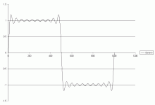
poobah said:This is what a 1 kHz squarewave looks like with frequency range limited to 20 khz.
Now... to get rid of that nasty ringing........................................................................ you have to ADD higher harmonics... beyond 20 kHz.
Wrong
TDA1541A external bias current
Hi JonHarrison,
TDA1541A chips have 2mA bias current:
No signal, 2mA current, maximum positive signal amplitude, 4mA current, maximum negative signal amplitude, 25nA current. If the TDA1541A internal current source drifts, all derived binary weighted currents change accordingly.
External bias current sources need to have very low drift, in order to provide DC coupling (external current source drift results in DC offset voltages).
If the external current source isn't fully linear (varies with TDA1541A output current), non-linear distortion is introduced, as the external bias current now fluctuates. It only takes fluctuations in the nA range to introduce bit errors.
Even if the TDA1541A bias current is zero, and bit errors aren't increased too much, I/V conversion is still required, while the AC voltage on the TDA1541A output should stay well below 25mV.
The TDA1541A was specifically designed to drive output current into virtual ground (OP-amp). By using 2mA bias current, signal zero crossing (0V) is shifted above OP-amp zero crossing (DC bias). This prevents OP-amp crossover distortion to affect low level signals.
DI8M uses two DAC groups, one group receives an inverted signal, the other a non-inverted signal. By converting this differential output signal into a single-ended signal, the DC component is cancelled, and the output signal amplitude is doubled.
Hi JonHarrison,
Sorry to bump this message but I think it got lost in discussions about other things and I'd be interested in hearing what people think about the idea.
TDA1541A chips have 2mA bias current:
No signal, 2mA current, maximum positive signal amplitude, 4mA current, maximum negative signal amplitude, 25nA current. If the TDA1541A internal current source drifts, all derived binary weighted currents change accordingly.
External bias current sources need to have very low drift, in order to provide DC coupling (external current source drift results in DC offset voltages).
If the external current source isn't fully linear (varies with TDA1541A output current), non-linear distortion is introduced, as the external bias current now fluctuates. It only takes fluctuations in the nA range to introduce bit errors.
Even if the TDA1541A bias current is zero, and bit errors aren't increased too much, I/V conversion is still required, while the AC voltage on the TDA1541A output should stay well below 25mV.
The TDA1541A was specifically designed to drive output current into virtual ground (OP-amp). By using 2mA bias current, signal zero crossing (0V) is shifted above OP-amp zero crossing (DC bias). This prevents OP-amp crossover distortion to affect low level signals.
DI8M uses two DAC groups, one group receives an inverted signal, the other a non-inverted signal. By converting this differential output signal into a single-ended signal, the DC component is cancelled, and the output signal amplitude is doubled.
I/V circuits
Hi panther5429,
Thanks for the compliments,
I haven't ordered professional PCBs for the new modules (UTOS1, UTOS2 and local reclocker) yet, that's why they are not listed on my website.
Yes, for PCB-only kits, it's on my website under downloads.
Prices for parts, assembled modules or complete products are available on request.
No, I stick with Op-amp I/V. I only needed to solve negative feedback loop instabilities. The noise-gain manipulation improved settling time, but increased distortion.
Turned out that LM4562 don't likes capacitive loads, so all I had to do is isolate all capacitive loads (compensation / filter caps and screened wires) from the LM4562 output by inserting 82 ... 100 Ohm series resistors.
Hi panther5429,
Thanks for the compliments,
Your webside can´t go the pace of Your progress
I haven't ordered professional PCBs for the new modules (UTOS1, UTOS2 and local reclocker) yet, that's why they are not listed on my website.
Is there any aktuell pricelist?
Yes, for PCB-only kits, it's on my website under downloads.
Prices for parts, assembled modules or complete products are available on request.
do You have something like this in mind?
No, I stick with Op-amp I/V. I only needed to solve negative feedback loop instabilities. The noise-gain manipulation improved settling time, but increased distortion.
Turned out that LM4562 don't likes capacitive loads, so all I had to do is isolate all capacitive loads (compensation / filter caps and screened wires) from the LM4562 output by inserting 82 ... 100 Ohm series resistors.
Re: I/V circuits
John, could you give us the schematic of UTOS as you did for another modules before? Thx.
-ecdesigns- said:
I haven't ordered professional PCBs for the new modules (UTOS1, UTOS2 and local reclocker) yet, that's why they are not listed on my website.
John, could you give us the schematic of UTOS as you did for another modules before? Thx.
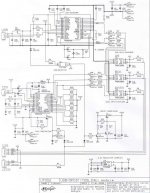
UTOS2 schematics
Hi ims,
I will try to attach the UTOS2 schematic first. diyAudio members can always email me for schematics.
It consists of a PCM2706 USB receiver and a CS8416 SPDIF receiver on one mall PCB.
The PCM2706 is bus powered (receives power from computer), and HPCL2630, dual high-speed opto-couplers are used for galvanic insulation. The opto-couplers are driven by 74HC14 buffers, and operate at low power levels. The opto-couplers support sample rates up to 96 KHz (CS8416).
The CS8416 I2S outputs also run through these opto-couplers (source selection). I use a small TOSLINK receiver module for SPDIF, but design is such that a high-quality pulse transformer can be added too (coax).
U3 (opto-coupler) signals the presence of the USB bus voltage and then swithes to USB automatically. The unused interface (USB or SPDIF) is powered down automatically, either by removing USB bus voltage, or the SPDIF power down circuit.
CS8416 receiver is straight-forward, it's runs in hardware mode, programmed to support I2S, 64BCK/WS, one's complement as required by the DI core. The required 3.3V is derived from a low-dropout voltage regulator.
The LED indicator signals the following:
USB (ON)
SPDIF (OFF)
No lock (flashing)
UTOS2 REQUIRES a reclocker, as opto-couplers increase jitter. So UTOS2 is followed by the completely redesigned local reclocker.
Due to the low jitter required (<2.7 ps RMS), I had to insert resistors of specific values in the clock distribution, and connect all IC shieldings to GND.
The IC shielding now also act as low impedance decoupling route, as I soldered a NPO / COG decoupling caps directly between the IC VCC pin and the copper shield. This also contributes to very low jitter levels.
Attachments
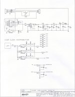
LRM schematics
Hi ims,
The DI8M / DI6(8*4), require very low jitter 1 / 352,800 / 2^19 / 2 = 2.7ps RMS.
so just connecting a PCM2706 or CS8416 receiver is NOT going to work. CS8416 clock jitter is specified at 200ps RMS typical, PCM2706 is even worse. So in order to achieve the required 2.7ps RMS, reclocking is always required.
The LRM reduces phase noise, but introduces some low amplitude correlated jitter in the process. Performance is similar to that of a synchronous reclocker.
The LRM schematics,
The low jitter 48 MHz master clock feeds the shift register through a 22R metal film resistor. The shift register is not reset like with the previous reclocker, but the output is inverted, and fed back to the second input. This results in a rotating bit pattern, fully synchronous with the master clock.
The master clock power supply is a shunt regulator (precision band-gap reference diode), programmed at 3.85V.
The module lay-out is extremely critical (HF), and required many redesigns to get a very low jitter amplitude with a jitter residual spectra that gives optimal sound quality.
BCK distribution was just as critical, by inserting resistors in the BCK signal path, jitter could be reduced at the both the TDA1541A clock inputs AND the master clock itself.
I also had to use special power supply bypassing on all ICs in the timing module. The copper shielding is now connected to the IC GND pin on one side, and a COG 100nF capacitor is connected between the IC power supply pin and the copper shield. The low impedance of the copper shield ensures short HF return paths.
Attachments
- Home
- Source & Line
- Digital Line Level
- Building the ultimate NOS DAC using TDA1541A