PS3 for TDA1541A
Hi
I am considering to use up-sampled 24bit 176.4kHz output of PlayStation3 for TDA1541A.
(But I do not have much money to buy them now )
)
It is not Non-oversamped ,but up-sampling function of PS3 is the best digital filter of any other hardware-digital filter, I think.
�iIts stop band attenuation is -320dB!! ex. df1704 : -115dB�j
I decide to use CS8416 why CS8416 is only a DIR I can get easly.
But CS8416 has some problems.
first ,it can not output 16bit I2S format.
second, its BCK is 11.2896 MHz. TDA1541A can accept lower than 6.4MHz.
I worked out a scheme to convert to .
I attatched the schematic file of EAGLE.
Could someone check it which work well or not?
<a href=http://proxy.f3.ymdb.yahoofs.jp/bc/44b65e06_8823/bc/%a5ޥ%a4%a5ɥ%ad%a5%e5%a5%e1%a5%f3%a5%c8/a.sch?BCpMTUHBludCrrP4>schematic</a>
I am sorry the schematic is hard to read and not compleated.
#It isnt licence violation to upload a schematic file of eagle
Hi
I am considering to use up-sampled 24bit 176.4kHz output of PlayStation3 for TDA1541A.
(But I do not have much money to buy them now
)It is not Non-oversamped ,but up-sampling function of PS3 is the best digital filter of any other hardware-digital filter, I think.
�iIts stop band attenuation is -320dB!! ex. df1704 : -115dB�j
I decide to use CS8416 why CS8416 is only a DIR I can get easly.
But CS8416 has some problems.
first ,it can not output 16bit I2S format.
second, its BCK is 11.2896 MHz. TDA1541A can accept lower than 6.4MHz.
I worked out a scheme to convert to .
I attatched the schematic file of EAGLE.
Could someone check it which work well or not?
<a href=http://proxy.f3.ymdb.yahoofs.jp/bc/44b65e06_8823/bc/%a5ޥ%a4%a5ɥ%ad%a5%e5%a5%e1%a5%f3%a5%c8/a.sch?BCpMTUHBludCrrP4>schematic</a>
I am sorry the schematic is hard to read and not compleated.
#It isnt licence violation to upload a schematic file of eagle
**** yahoo briefcase!!!
http://briefcase.yahoo.co.jp/bc/ope....src=bc&.done=http%3a//briefcase.yahoo.co.jp/
is this ok?
http://briefcase.yahoo.co.jp/bc/ope....src=bc&.done=http%3a//briefcase.yahoo.co.jp/
is this ok?
PCM2706/7 power supply
Hi Radian,
I already tried PCM2706 self-powered mode, if no reclocker is used, it could improve performance to some extent.
Problem might be noise / interference from the computer reaching the DAC electronics, causing increased jitter / noise.
But I use a different scheme for my USBDI2S interface, PCM2706 GND and DAC GND are separated (not connected). I use differential buffers to route the I2S signals, common noise is rejected. These differential signals are not referenced to GND. The DI2S receiver has a separate 5V power supply. This is very different from standard PCM2706/07 applications, and it greatly reduces noise / interference.
The USBDI2S power supply is heavily filtered & decoupled, even down to chip level. The master clock oscillator power supply (most critical) has 100nF soldered directly to the SMD module power supply pins, a miniature 330uF tantalium cap is mounted close to the module (in the IC socket) and a 22R / 430uF filter is located on the PCB. On top of that, cascaded Murata power supply filters are used.
The signal scheme is as follows:
USB (computer) > 5m USB interlink > PCM2706 bus powered (powered by computer) > reclocker (clean signal) > I2S > DI2S > I2S (source selection) > clock buffer (NC7SZ125M5 / NC7SZ04M5) > DAC groups.
Hi Radian,
I would still suggest trying the PCM2707 in self powered mode to see for yourself if the junk of the USB power is affecting the sound or not.
I already tried PCM2706 self-powered mode, if no reclocker is used, it could improve performance to some extent.
Problem might be noise / interference from the computer reaching the DAC electronics, causing increased jitter / noise.
But I use a different scheme for my USBDI2S interface, PCM2706 GND and DAC GND are separated (not connected). I use differential buffers to route the I2S signals, common noise is rejected. These differential signals are not referenced to GND. The DI2S receiver has a separate 5V power supply. This is very different from standard PCM2706/07 applications, and it greatly reduces noise / interference.
The USBDI2S power supply is heavily filtered & decoupled, even down to chip level. The master clock oscillator power supply (most critical) has 100nF soldered directly to the SMD module power supply pins, a miniature 330uF tantalium cap is mounted close to the module (in the IC socket) and a 22R / 430uF filter is located on the PCB. On top of that, cascaded Murata power supply filters are used.
The signal scheme is as follows:
USB (computer) > 5m USB interlink > PCM2706 bus powered (powered by computer) > reclocker (clean signal) > I2S > DI2S > I2S (source selection) > clock buffer (NC7SZ125M5 / NC7SZ04M5) > DAC groups.
Hi Radian.
The murata filters are nothing special, just two ferrite beads and a capacitor of 10nF. I tried PCM2706 self-powered mode, even tested battery power supplies, but the main problem doesn't seem to be the power supply in this case, it's the digital circuits attached to it that seem to pollute it heavily.
By interrupting USB ground and DAC ground, and using differential buffers for all I2S signals, significant noise attenuation was already achieved.
The easiest way to do this, is by using bus powered mode. Possible extra timing jitter on BCK is irrelevant at this stage since BCK is reclocked later.
So the USB power supply doesn't worry me that much, what needs more attention is the noise / interference generated by the ICs used in the USBDI2S module. Even the I2S signal itself will already cause significant power supply pollution.
So I tried to attenuate noise emerging from each separate IC, by using a dedicated power supply filter for each IC. These filters work both ways, they attenuate noise produced from the chips, and they attenuate noise already present on the power supply rail.
Then it turned out that the ICs also emitted a certain amount of EMI (Electro Magnetic Interference), just think about the vast amount of transistors that are switching in a chip like the PCM2706. So even if the power supply is correctly filtered, interference would still occur. The EMI induces currents in the ground planes and PCB traces, injecting more noise (the ICs act as HF transmitters, the PCB traces act as antennas). This is the reason why I also put copper foil EMC screening around each chip, this will at least attenuate the EMC emitted from the ICs a bit.
So unfortunately signals usually don't follow the neat lines drawn in the schematics. Using super regulators doesn't necessarily mean that all power supply problems are automatically solved.
PCB lay-out, and EMC screening for example will have a major impact on circuit performance, especially with these timing-sensitive circuits.
t's hard to believe that three caps and a Murata filter are able to clean up a USB bus.
Is it a secret what Murata filter you used?
The murata filters are nothing special, just two ferrite beads and a capacitor of 10nF. I tried PCM2706 self-powered mode, even tested battery power supplies, but the main problem doesn't seem to be the power supply in this case, it's the digital circuits attached to it that seem to pollute it heavily.
By interrupting USB ground and DAC ground, and using differential buffers for all I2S signals, significant noise attenuation was already achieved.
The easiest way to do this, is by using bus powered mode. Possible extra timing jitter on BCK is irrelevant at this stage since BCK is reclocked later.
So the USB power supply doesn't worry me that much, what needs more attention is the noise / interference generated by the ICs used in the USBDI2S module. Even the I2S signal itself will already cause significant power supply pollution.
So I tried to attenuate noise emerging from each separate IC, by using a dedicated power supply filter for each IC. These filters work both ways, they attenuate noise produced from the chips, and they attenuate noise already present on the power supply rail.
Then it turned out that the ICs also emitted a certain amount of EMI (Electro Magnetic Interference), just think about the vast amount of transistors that are switching in a chip like the PCM2706. So even if the power supply is correctly filtered, interference would still occur. The EMI induces currents in the ground planes and PCB traces, injecting more noise (the ICs act as HF transmitters, the PCB traces act as antennas). This is the reason why I also put copper foil EMC screening around each chip, this will at least attenuate the EMC emitted from the ICs a bit.
So unfortunately signals usually don't follow the neat lines drawn in the schematics. Using super regulators doesn't necessarily mean that all power supply problems are automatically solved.
PCB lay-out, and EMC screening for example will have a major impact on circuit performance, especially with these timing-sensitive circuits.
[As noted earlier on this thread, I think two criteria must be met in order to achieve optimal performance when using digital sound sources:
1) Data must be bit correct, or at least with as few errors as possible. Most CD, CDROM, DVD transports will manage to output the correct data (after CRC correction), regardless if they are cheap units like the ones used in computers, or expensive High-end transports.
Cheers,
John [/B]
John
Looking at PC based system using front end: Vista OS and XXhighEnd Player (latest version http://www.phasure.com/index.php). Do you know of anybody using the TDA1541A DAC design who also uses or has recently tried that PC front end and player?
Thanks
Frank
Hi operafollower,
It can output I2S 24bit in hardware mode. The TDA1541A seems to have no problem with this (tested this earlier this year).
I used OLRCK (WS) pin 28, OSCLK (BCK) pin 27 and SDOUT (DATA) pin 26. I got 2.8224 MHz bit clock (BCK), so again no problem here. RMCK (pin 24) outputs 128fs (5.6448 MHz) or 256fs (11.2896 MHz) depending on HW settings, but I didn't use this output (NOS DAC).
Sorry I wasn't able to view your schematic diagram.
But CS8416 has some problems. first ,it can not output 16bit I2S format.
It can output I2S 24bit in hardware mode. The TDA1541A seems to have no problem with this (tested this earlier this year).
second, its BCK is 11.2896 MHz. TDA1541A can accept lower than 6.4MHz.
I used OLRCK (WS) pin 28, OSCLK (BCK) pin 27 and SDOUT (DATA) pin 26. I got 2.8224 MHz bit clock (BCK), so again no problem here. RMCK (pin 24) outputs 128fs (5.6448 MHz) or 256fs (11.2896 MHz) depending on HW settings, but I didn't use this output (NOS DAC).
Sorry I wasn't able to view your schematic diagram.
Hi guys,
Yesterday I played around with my new-old 20MHz scope trying to figure out why my TVC seems to be noisy (I suspect HF ringing as described on Stevens&Billington's site on certain conditions).
System: laptop->USB->DI16 with Doede's USB module->TVC. I use unbalanced to balanced cable but I forgot to disconnect the shield to PIN1 (by memory).
DI16 output is clean and continuous up to 20KHz. The secondaries are difficult to check: I use a test CD with 10 second samples so it's really difficult to measure sometimes because of lower Voltage I have to calibrate (red button; sorry I'm new to scopes) or I end with 3 simultaneous parallel curves. The problem is that at idle I detect a 10mV 5MHz signal that disappears when laptop is off: anyone knows what is this signal.
Ah! I forgot, signal does not change when changing attenuation and is the same on the TVC primaries...
Thanks,
M
Yesterday I played around with my new-old 20MHz scope
trying to figure out why my TVC seems to be noisy (I suspect HF ringing as described on Stevens&Billington's site on certain conditions).System: laptop->USB->DI16 with Doede's USB module->TVC. I use unbalanced to balanced cable but I forgot to disconnect the shield to PIN1 (by memory).
DI16 output is clean and continuous up to 20KHz. The secondaries are difficult to check: I use a test CD with 10 second samples so it's really difficult to measure sometimes because of lower Voltage I have to calibrate (red button; sorry I'm new to scopes) or I end with 3 simultaneous parallel curves. The problem is that at idle I detect a 10mV 5MHz signal that disappears when laptop is off: anyone knows what is this signal.
Ah! I forgot, signal does not change when changing attenuation and is the same on the TVC primaries...
Thanks,
M
OK Tubee, I understand that. I will disconnect cable's shield at TVC's input and RC filter to ground the PIN1 input and see what happens. Anyway a +/-5MHz sine about 10mV pp, considering the secondaries low potential might affect the amps...or it may get filtered at amp's input circuit instead.
I'll check TVC with square waves instead with my new-old function generator ...and also, if time allows, I will take a look at DI16 circuits...and at my amps, and my....and my... 
Sorry for the OT
Cheers,
M
I'll check TVC with square waves instead with my new-old function generator
...and also, if time allows, I will take a look at DI16 circuits...and at my amps, and my....and my... Sorry for the OT
Cheers,
M
Re: DEM clock
Thanks ecdesigns for greatful and full sharing work. I took many tweak or idea here. The dac I use is a simple CS8414/TDA1541A powered by few jung like regulator, using a jfet D1 as I/V (with vishay bulk foil R), a simple shared reclock board for BCK and the SA7220 (allowing to bypass the SA7220 internal clock).
This shared clock now provide the 352.8 Khz for the DEM Clock. I don't have any scope but listening sessions leads me to the conclusion that it's really worth the case:
Sound becomes clearer, what was really noticeable (on my system) is the air it provides between instruments . Due to it, the soundstage turns accurate, it's easier for instance to follow the background bass player... voice remains unprojected but are more detailed. To conclude Joe Sample piano lays precisely in the background while R. Crawford sings clearly in front of me...
I can't imagine what it could gave with 8x 1541A
-ecdesigns- said:Hi rtd,
Use the upper schematic diagram (BCK 2.8224 MHz)
Connect the DEM clock to 74HC161 pin 11 (pin next to the two +5V connections).
This will divide the 5.6448 MHz by 16 and provide the 352.8 KHz DEM clock
Thanks ecdesigns for greatful and full sharing work. I took many tweak or idea here. The dac I use is a simple CS8414/TDA1541A powered by few jung like regulator, using a jfet D1 as I/V (with vishay bulk foil R), a simple shared reclock board for BCK and the SA7220 (allowing to bypass the SA7220 internal clock).
This shared clock now provide the 352.8 Khz for the DEM Clock. I don't have any scope but listening sessions leads me to the conclusion that it's really worth the case:
Sound becomes clearer, what was really noticeable (on my system) is the air it provides between instruments
. Due to it, the soundstage turns accurate, it's easier for instance to follow the background bass player... voice remains unprojected but are more detailed. To conclude Joe Sample piano lays precisely in the background while R. Crawford sings clearly in front of me... I can't imagine what it could gave with 8x 1541A
Local reclocker
Hi all,
Finally another update,
This one was initiated by onnosr, telling me he heard slight performance differences between USBDI2S module and SPDIFDI2S module.
This puzzled me a bit since both reclockers used identical reclock circuits, except for the SPDIFDI2S module being connected to a clean 5V power supply.....
The BCK clocking scheme bugged me for some time, I also wasn't happy using multiple reclockers. So I decided it was time to improve this.
This weekend I designed / installed the local reclocker. The reclocker is placed directly on the DI16 / DI8M core PCB to ensure shortest BCK signal path, it reclocks BCK from both USB / PCM2706, and DI2S. It provides an extreme low jitter clock directly at the DAC chip inputs. The existing reclockers on both USBDI2S and SPDIFDI2S modules were removed / bypassed. I put a custom 12 MHz oscillator in the USBDI2S module (74HC161 IC socket) for PCM2706 clock.
The clocking scheme has been simplified / improved:
Old situation:
USB > PCM2706 > reclocker > I2S > DI2S > I2S > I2S interlink > clock buffer > DAC chips
DI2S > I2S > I2S interlink > clock buffer > DAC chips (no reclocking)
note: The DI2S buffers are used to attenuate common interference, and provide I2S source selection.
New situation:
USB > I2S > DI2S > I2S > reclocker > clock buffer > DAC chips
DI2S > I2S > reclocker > clock buffers > DAC chips
Note: both digital audio sources are now reclocked. The reclocker can now run on an external clean power supply (no longer connected to USB power supply).
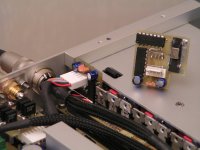
The photograph shows the local reclocker in my DI 8M reference DAC, another reclocker is placed on the heatsink for a better view. This reclocker can also be used with the DI 16.
Measurements:
The oscillograms taken directly from the TDA1541A chip BCK inputs show very clean rasor-sharp transients, now it's no longer possible to measure the jitter with my oscilloscope, even after minimum brightness setting and focus fine-adjust.
First impressions:
The improvement is immediately audible, no direct comparisons necessary for this mod. The sound-stage is wider, sound is smoother, cleaner and more detailed than before. Even at low volume settings the sound quality is exceptionally clear and detailed.
Hi all,
Finally another update,
This one was initiated by onnosr, telling me he heard slight performance differences between USBDI2S module and SPDIFDI2S module.
This puzzled me a bit since both reclockers used identical reclock circuits, except for the SPDIFDI2S module being connected to a clean 5V power supply.....
The BCK clocking scheme bugged me for some time, I also wasn't happy using multiple reclockers. So I decided it was time to improve this.
This weekend I designed / installed the local reclocker. The reclocker is placed directly on the DI16 / DI8M core PCB to ensure shortest BCK signal path, it reclocks BCK from both USB / PCM2706, and DI2S. It provides an extreme low jitter clock directly at the DAC chip inputs. The existing reclockers on both USBDI2S and SPDIFDI2S modules were removed / bypassed. I put a custom 12 MHz oscillator in the USBDI2S module (74HC161 IC socket) for PCM2706 clock.
The clocking scheme has been simplified / improved:
Old situation:
USB > PCM2706 > reclocker > I2S > DI2S > I2S > I2S interlink > clock buffer > DAC chips
DI2S > I2S > I2S interlink > clock buffer > DAC chips (no reclocking)
note: The DI2S buffers are used to attenuate common interference, and provide I2S source selection.
New situation:
USB > I2S > DI2S > I2S > reclocker > clock buffer > DAC chips
DI2S > I2S > reclocker > clock buffers > DAC chips
Note: both digital audio sources are now reclocked. The reclocker can now run on an external clean power supply (no longer connected to USB power supply).
The photograph shows the local reclocker in my DI 8M reference DAC, another reclocker is placed on the heatsink for a better view. This reclocker can also be used with the DI 16.
Measurements:
The oscillograms taken directly from the TDA1541A chip BCK inputs show very clean rasor-sharp transients, now it's no longer possible to measure the jitter with my oscilloscope, even after minimum brightness setting and focus fine-adjust.
First impressions:
The improvement is immediately audible, no direct comparisons necessary for this mod. The sound-stage is wider, sound is smoother, cleaner and more detailed than before. Even at low volume settings the sound quality is exceptionally clear and detailed.
Attachments
That is great news John.
Now we can even improve USB module or just added after.
MaxLorenz you were right about 8X4 mode.
My DI16 8X4 performing very well. Clear sound, much better than DI16 basic.
I had hard time to make alu towers by hand (2-3 weeks), still i used thermal paste and silicon pads to get good thermal contact.
CNC machine would be best for that work.
But now enjoying.
I am completely enthusiastic about this DAC, i ordered also TUBE DIF PCBs.
regards,
Bostjan
Hi John, hi Bostjan
John, why are you so cruel? Now you have to guide about how to mod my setup.
As I understand, now you have two 12Mhz clocks, right? One for PCM2706 and one for BCK. Why don't we use a 11.28Mhz for BCK, instead, since it has its own low noise PS???
Ah! At last! I felt so lonely
Well, it is true that 1543 is a low resolution DAC. With 32 DACs you gain in resolution, while retaining that warmth and intimacy that NOS gives.
I would love to be able to get one DI8, though. But I'm risking divorce here (3 DIY systems; 5 digital sources; planning even bigger horn speakers)
About, heatsinks for the towers, lovely job, ain't it?
I'm sure there will be a cheap alternative in the future
Cheers,
M
PS: I have here 20uF, SMD tantalum caps and X7R smd 0603 caps that I could use as PS bypass for the towers (bottom side) instead of the stock setup...what do you think John?
John, why are you so cruel? Now you have to guide about how to mod my setup.
As I understand, now you have two 12Mhz clocks, right? One for PCM2706 and one for BCK. Why don't we use a 11.28Mhz for BCK, instead, since it has its own low noise PS???
MaxLorenz you were right about 8X4 mode. My DI16 8X4 performing very well. Clear sound, much better than DI16 basic.
I had hard time to make alu towers by hand (2-3 weeks), still i used thermal paste and silicon pads to get good thermal contact.
CNC machine would be best for that work.
But now enjoying.
Ah! At last! I felt so lonely
Well, it is true that 1543 is a low resolution DAC. With 32 DACs you gain in resolution, while retaining that warmth and intimacy that NOS gives.
I would love to be able to get one DI8, though. But I'm risking divorce here
(3 DIY systems; 5 digital sources; planning even bigger horn speakers)About, heatsinks for the towers, lovely job, ain't it?
I'm sure there will be a cheap alternative in the future
Cheers,
M
PS: I have here 20uF, SMD tantalum caps and X7R smd 0603 caps that I could use as PS bypass for the towers (bottom side) instead of the stock setup...what do you think John?
-ecdesigns-:
I'm getting ready to make the plunge! I have half the parts and will be placing an order in a week for the rest. I just had the chance to open up my current transport and peek inside... Unfortuantely, I'm not sure it is compatible with the Philips i2s standard. However, I do not have the expertise to determine for sure.
The chip used is Panasonic MN66271RA. Here is a datasheet:
http://www.ortodoxism.ro/datasheets/panasonic/MN66271RA.pdf
There are no timing diagrams. Pins 1,2,3 are available, but very small pads They are BCLK, LRCK, SRDATA. There are a few frequency adjustment pins and a number of clocks present as well. Is there a hope for this working, or should I sell this transport and look for a new one that will be easier to modify?
Thank you!
I'm getting ready to make the plunge! I have half the parts and will be placing an order in a week for the rest. I just had the chance to open up my current transport and peek inside... Unfortuantely, I'm not sure it is compatible with the Philips i2s standard. However, I do not have the expertise to determine for sure.
The chip used is Panasonic MN66271RA. Here is a datasheet:
http://www.ortodoxism.ro/datasheets/panasonic/MN66271RA.pdf
There are no timing diagrams. Pins 1,2,3 are available, but very small pads
They are BCLK, LRCK, SRDATA. There are a few frequency adjustment pins and a number of clocks present as well. Is there a hope for this working, or should I sell this transport and look for a new one that will be easier to modify?Thank you!
Re: The jitter frequency component that causes sound quality degradation
Hi ecdesigns.
I just read through this very interesting thread and I'm think that I will make this DAC.
But I have questions about the above statement.
Can you define "low amplitude phase noise" because in your diagram you show it as full amplitude random timing irregularities.
Can you describe how this phase noise disrupts high feedback amps differently from the asynchronous clocking deviation that you say does not disrupt them. The only things that I am aware of that disrupt feedback amps are frequencies above that which a circuit can handle.
My guess is that the low feedback circuit is simply smoothing over the HF noise problem while the high feedback circuit is having a try at resolving an input signal which it cannot handle and is it therefore making a mess of.
but why do "random timing irregularities" create a more challenging task for o/p stages than asynchronous re-clocking timing irregularities - it does not seem logical to me.
I do tend to believe that you have made a rather special DAC and I am very interested to listen to it. My question is why is it good ?
I can understand that eradicating the ringing present with oversampling is a big advantage because for me ringing = HF noise and noise is No1 enemy of high fidelity reproduction but at present this whole timing / clocking issue is a mystery to me ( unless we simply ascribe it to being a psycho acoustic phenomena ).
cheers
mike
-ecdesigns- said:
But tests I conducted showed that the low amplitude phase noise causes most problems. This was verified by both measurements and listening tests. It turns out that these very small phase deviations disrupt feedback loops in analog stages (DAC, pre-amplifier, power amplifier). Simple comparison tests between two power amps of the same type, one with high negative feedback, the other with significant lower feedback showed that the one with highest feedback produced sound degradation very similar to increased phase noise.
So I think that the jitter related sound degradation is primarily caused by disruption of analog circuits / feedback loops , rather than changing absolute sample timing.
Hi ecdesigns.
I just read through this very interesting thread and I'm think that I will make this DAC.
But I have questions about the above statement.
Can you define "low amplitude phase noise" because in your diagram you show it as full amplitude random timing irregularities.
Can you describe how this phase noise disrupts high feedback amps differently from the asynchronous clocking deviation that you say does not disrupt them. The only things that I am aware of that disrupt feedback amps are frequencies above that which a circuit can handle.
My guess is that the low feedback circuit is simply smoothing over the HF noise problem while the high feedback circuit is having a try at resolving an input signal which it cannot handle and is it therefore making a mess of.
but why do "random timing irregularities" create a more challenging task for o/p stages than asynchronous re-clocking timing irregularities - it does not seem logical to me.
I do tend to believe that you have made a rather special DAC and I am very interested to listen to it. My question is why is it good ?
I can understand that eradicating the ringing present with oversampling is a big advantage because for me ringing = HF noise and noise is No1 enemy of high fidelity reproduction but at present this whole timing / clocking issue is a mystery to me ( unless we simply ascribe it to being a psycho acoustic phenomena ).
cheers
mike
Share reclock board
Hi rtd,
I also have a simple SA7220/CS8414/TDA1541A DAC and am interested in your "simple shared reclock board for BCK and the SA7220 (allowing to bypass the SA7220 internal clock)". Can you share with me more information on this?
Thanks & Best Regards
S K
Hi rtd,
I also have a simple SA7220/CS8414/TDA1541A DAC and am interested in your "simple shared reclock board for BCK and the SA7220 (allowing to bypass the SA7220 internal clock)". Can you share with me more information on this?
Thanks & Best Regards
S K
Hi mikelm
With low amplitude phase noise, I refer to RANDOM phase fluctuations (phase noise) up to approx. 1000ps RMS. Most asynchronous reclockers introduce repetitive / predictive phase fluctuations, provided the reclockers master clock has low phase noise, the master clock frequency will also limit jitter bandwidth. Example, an 48 MHz asynchronous reclocker needs two clock periods before the output signal can change, so the reclocked signal can only change after at least 42ns intervals.
So there is a big difference in jitter spectra (noise vs square wave)
The shiftregister reclocker works much more accurate than a plain asynchronous reclocker. The newest version manages to exactly align 99.96% of the output pulses, using a 48MHz masterclock. A plain asynchronous reclocker can only align approx. 50%.
It all boils down to higher harmonics that exceed the amplifiers bandwidth, disrupting the (local) feedback loop, introducing (non-linear / dynamic) distortion. Jitter adds extra harmonics over a large bandwidth, this harmonics pattern fluctuates randomly.
And it's not only amplifiers, all circuits and components that need to process the audio signal, must be able to cope with both the audio signal AND the accompanied higher harmonics. By this I mean it should respond fully linear over the required bandwidth, adding no extra distortion.
Problems with higher harmonics occur in the D/A converter itself, I/V converter, differential amplifiers, and analogue reconstruction filter.
It would help if higher harmonics could be reduced to start with. This is exactly what a NOS DAC does (remember the higher harmonics also have to pass the analogue part of D/A conversion stage). Band limiting / filtering hasn't occurred yet in this stage.
Despite OS brickwall filtering, it's the analogue reconstruction filter that actually attenuates higher harmonics to some extent. The un-attenuated higher harmonics already caused havoc in the D/A, I/V, differential stages and analogue reconstruction filter by then.
Because they are random, it's very difficult to "average" between these fluctuations. Repetitive fluctuations can be averaged more easily.
I explained this already on this thread. But I will make a short list:
- No analogue filters (extreme low phase distortion)
- Direct interpolation (increases both time and amplitude resolution)
- Zero ringing
- Extreme low jitter timing signal at DAC timing inputs (local reclocker)
- Multiple DAC chips in parallel (reduces bit errors)
- Balanced design (cancels common interference)
- Very high amplitude internal signal levels (noise immunity)
- Accepts USB, I2S, DI2S and SPDIF / TOSLINK (connects to most digital sources)
- Full galvanic insulation between source and DAC (new digital front-ends), prevents ground loops and blocks source noise
- Unique mixed-mode output (balances both odd and even harmonics)
- Modular design (allows for easy future upgrades)
- Selected components (low level tuning)
- Class A operation of operational amplifiers (less crossover distortion)
When a 1 KHz square wave signal is band limited at 20 KHz (brickwall anti aliasing filter), prior to sampling, it already shows ringing. After the D/A process in the DAC it still shows ringing. However, the reproduced 1 KHz square wave differs from the original signal before anti aliasing.
Depending on how our hearing interprets this band limited signal, it might sound different from the original square wave. It's likely that more complex audio signals make the effects of ringing as a result of band limiting more audible.
Ringing could be reduced by significantly increasing both bandwidth and sample rate, this however isn't very practical for the reasons I already indicated.
The whole timing and clocking issue results in 7 or 15 linear interpolated samples placed between the existing samples in real-time, (Direct Interpolation).
This increases both time resolution (from 44.1 KHz to 352.8 or 706.5 KHz), and amplitude resolution (from 16 bits to 19 or 20 bits, however this depends on tolerances).
In the process it also acts as a linear filter, effectively attenuating higher harmonics, but since it's no brickwall filter, intermodulations with fs still occur, as fs is too close to the audio range. However, higher harmonics are effectively attenuated. This is the reason why I can leave-out the analogue filter, similar to the Trinity DAC.
Because I use multiple DAC chips, each chip has to process less higher harmonics, as it runs at fs (NOS mode), and part of the interpolation takes place in the analogue domain as well.
Can you define "low amplitude phase noise" because in your diagram you show it as full amplitude random timing irregularities.
With low amplitude phase noise, I refer to RANDOM phase fluctuations (phase noise) up to approx. 1000ps RMS. Most asynchronous reclockers introduce repetitive / predictive phase fluctuations, provided the reclockers master clock has low phase noise, the master clock frequency will also limit jitter bandwidth. Example, an 48 MHz asynchronous reclocker needs two clock periods before the output signal can change, so the reclocked signal can only change after at least 42ns intervals.
So there is a big difference in jitter spectra (noise vs square wave)
The shiftregister reclocker works much more accurate than a plain asynchronous reclocker. The newest version manages to exactly align 99.96% of the output pulses, using a 48MHz masterclock. A plain asynchronous reclocker can only align approx. 50%.
My guess is that the low feedback circuit is simply smoothing over the HF noise problem while the high feedback circuit is having a try at resolving an input signal which it cannot handle and is it therefore making a mess of.
It all boils down to higher harmonics that exceed the amplifiers bandwidth, disrupting the (local) feedback loop, introducing (non-linear / dynamic) distortion. Jitter adds extra harmonics over a large bandwidth, this harmonics pattern fluctuates randomly.
And it's not only amplifiers, all circuits and components that need to process the audio signal, must be able to cope with both the audio signal AND the accompanied higher harmonics. By this I mean it should respond fully linear over the required bandwidth, adding no extra distortion.
Problems with higher harmonics occur in the D/A converter itself, I/V converter, differential amplifiers, and analogue reconstruction filter.
It would help if higher harmonics could be reduced to start with. This is exactly what a NOS DAC does (remember the higher harmonics also have to pass the analogue part of D/A conversion stage). Band limiting / filtering hasn't occurred yet in this stage.
Despite OS brickwall filtering, it's the analogue reconstruction filter that actually attenuates higher harmonics to some extent. The un-attenuated higher harmonics already caused havoc in the D/A, I/V, differential stages and analogue reconstruction filter by then.
but why do "random timing irregularities" create a more challenging task for o/p stages than asynchronous re-clocking timing irregularities - it does not seem logical to me.
Because they are random, it's very difficult to "average" between these fluctuations. Repetitive fluctuations can be averaged more easily.
I do tend to believe that you have made a rather special DAC and I am very interested to listen to it. My question is why is it good ?
I explained this already on this thread. But I will make a short list:
- No analogue filters (extreme low phase distortion)
- Direct interpolation (increases both time and amplitude resolution)
- Zero ringing
- Extreme low jitter timing signal at DAC timing inputs (local reclocker)
- Multiple DAC chips in parallel (reduces bit errors)
- Balanced design (cancels common interference)
- Very high amplitude internal signal levels (noise immunity)
- Accepts USB, I2S, DI2S and SPDIF / TOSLINK (connects to most digital sources)
- Full galvanic insulation between source and DAC (new digital front-ends), prevents ground loops and blocks source noise
- Unique mixed-mode output (balances both odd and even harmonics)
- Modular design (allows for easy future upgrades)
- Selected components (low level tuning)
- Class A operation of operational amplifiers (less crossover distortion)
I can understand that eradicating the ringing present with oversampling is a big advantage because for me ringing = HF noise and noise is No1 enemy of high fidelity reproduction but at present this whole timing / clocking issue is a mystery to me ( unless we simply ascribe it to being a psycho acoustic phenomena ).
When a 1 KHz square wave signal is band limited at 20 KHz (brickwall anti aliasing filter), prior to sampling, it already shows ringing. After the D/A process in the DAC it still shows ringing. However, the reproduced 1 KHz square wave differs from the original signal before anti aliasing.
Depending on how our hearing interprets this band limited signal, it might sound different from the original square wave. It's likely that more complex audio signals make the effects of ringing as a result of band limiting more audible.
Ringing could be reduced by significantly increasing both bandwidth and sample rate, this however isn't very practical for the reasons I already indicated.
The whole timing and clocking issue results in 7 or 15 linear interpolated samples placed between the existing samples in real-time, (Direct Interpolation).
This increases both time resolution (from 44.1 KHz to 352.8 or 706.5 KHz), and amplitude resolution (from 16 bits to 19 or 20 bits, however this depends on tolerances).
In the process it also acts as a linear filter, effectively attenuating higher harmonics, but since it's no brickwall filter, intermodulations with fs still occur, as fs is too close to the audio range. However, higher harmonics are effectively attenuated. This is the reason why I can leave-out the analogue filter, similar to the Trinity DAC.
Because I use multiple DAC chips, each chip has to process less higher harmonics, as it runs at fs (NOS mode), and part of the interpolation takes place in the analogue domain as well.
- Home
- Source & Line
- Digital Line Level
- Building the ultimate NOS DAC using TDA1541A