Bernhard said:Another variation of linear interpolation came to my mind, did not think it through...
It could use a 8x os filter to produce "good" new samples.
A decade counter distributes the samples to 8 DACs in a ring configuration.
The result is a data update rate of 44,1 kHz for each DAC like in non os, and overlap of the DACs is the same as with linear interpolation but it uses true ( interpolated )samples.
Any good ?
Nobody ?
Bernhard said:
Nobody ?
Are you sure you want me to comment?
rfbrw said:
Are you sure you want me to comment?
rfbrw, be nice...
Phil wrote:
Yes!
Hypex' UCD400 amps, DC coupled, fed with DIY 4*TDA1543 through TVC: my ten dollar DAC sounds awsome save on HF! I believe it is aliasing.
(but I am the first to accept that I don't know a sh*** about this, so big brothers, no need to recommend other hobby )
)
Ecdesigns wrote:
Thanks John, but 3 more opamps on signal path? I prefer to wait for the "pièce de resistance"
Cheers
M
So, those with unfiltered NOS DACs, does this ultrasonic hash and resultant aliasing bother you?
Yes!
Hypex' UCD400 amps, DC coupled, fed with DIY 4*TDA1543 through TVC: my ten dollar DAC sounds awsome save on HF! I believe it is aliasing.
(but I am the first to accept that I don't know a sh*** about this, so big brothers, no need to recommend other hobby
)Ecdesigns wrote:
The aliasing can be attenuated, by using a 8th order Butterworth filter (I attached the schematic diagram).
Thanks John, but 3 more opamps on signal path? I prefer to wait for the "pièce de resistance"
But perceived subjective roll-off depends greatly on output cap chosen, IMHO. That is why I prefer balanced DC coupled output...The experienced roll-of of treble in nonos is normal due the frequency output of dac alone.
Cheers
M
Yes i have tube amplification too, pre-amp and voltage stage of power-amp, to speakers Fets. And no feedback, only local. But the simple 10 W JHL transistor monoblocks used before didn't have trouble with the non-os sound either (because of limited bandwith of the used 2N3055's?)
Hi MGH, tubee,
Most tube amplifiers will easily reproduce past 40 KHz. Tubee, if you used real 2N3055's, they had a -3dB down point of 19 KHz. They were intended for regulator pass elements mounted off board. That's why the low cut off frequency. I hate that transistor in audio!
Anyway, whether you heard it or not, you probably had artifacts showing up in your passband. Every non-linear element is a type of mixer. Tubes and transistors quality. Welcome to sum and difference plus your two fundamentals.
-Chris
Yes,
I use a dual TDA1541 DAC fed from a PC where the source is upsampled to 88.2khz with a 4th order output filter. The upsampled signal sounds cleaner at the top end, and removes the sinc rolloff you get with NOS which gives it more air.
I much prefer the upsampling to 44.1Khz at least with this setup (MOSFET amp).
Regards,
Dean
Off topic here, but its audio anyway.
Yes i know there are better subsitutes for the good old workhorse 2N3055, but the amps where made for an experiment until hybrid was ready.
Here they are, about 14 cm high monoblocks:
http://img213.imageshack.us/my.php?image=jlhamp9by.jpg
should try better transistors but now used hybrid amp sounds very good.
In search for datasheets of Yamaha YM 3414, 3613 and 3619
( Anybody has a datasheet or part of schematic of CDX-1100 or CDX-5000 containing YM3613 dither chip ? )
I found this:
http://www.aes.org/e-lib/browse.cfm?elib=4820
I will not download the article for 20 bucks as my analyzer has already told me the whole story.
( Anybody has a datasheet or part of schematic of CDX-1100 or CDX-5000 containing YM3613 dither chip ? )
I found this:
http://www.aes.org/e-lib/browse.cfm?elib=4820
Are D/A Converters Getting Worse?
A properly dithered 16-bit digital audio storage system with accurate analog-to-digital (A/D) and digital-to-analog (D/A) converters will outperform any analog storage medium in existence. With reasonable accurate converters, such a system performs and measures well at high levels. Its low-level behavior, however, is vitally dependent upon the small-signal differential linearity of the A/D and D/A converters used. Only if nonlinearities are held to tight tolerances can the performance come close to theoretical perfection, and the system not display low-level distortions. This problem is exacerbated by the fact that most converters display their worse differential nonlinearity at zero level, in the center of their range. We discuss here some of the problems in the D/A converter system design, including the digital filter of interpolating D/A systems (so-called "oversampling" D/As), and display measurements made on compact disc players of assorted vintages.
We find that the small-signal accuracy of the D/A systems of many currently available CD players is worse than that of models of a few years ago, and this applies even to some of the most expensive machines.
The arithmetic design of many of the digital filter circuits in use is also suboptimal.
We make the case that some of these defects are of sufficient magnitude to audibly degrade musical programs, and that proper low-level measurements including the use of dithered test tones should be used in the assessment of D/A converter systems.
I will not download the article for 20 bucks as my analyzer has already told me the whole story.
Re: NOS DAC filter / reclocker
Hello EC designs,
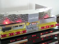
i have followed this thread from the begining and as i am planning to visit your counrty next month i wonder if i could pay you a visit and listened to the octal dac and the resonators.
My email address is marmatsouris@yahoo.com
many thanks
Hello EC designs,
i have followed this thread from the begining and as i am planning to visit your counrty next month i wonder if i could pay you a visit and listened to the octal dac and the resonators.
My email address is marmatsouris@yahoo.com
many thanks
Bernhard said:No, it is an IC in front of the DF and Dither is written on the pcb beside it. Looks like the data is dithered before entering the DF.
All sounds rather dubious to me especially as the YM3613 is a SPDIF transmitter
Bernhard said:Ups, so DIT means Digital Transmitter... Didn't know they had a special chip for that.
Yes, there are quite a few.
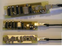
USB to I2S module completed
Hi all,
Project update,
Finally, the USB to I2S module is ready. It's a compact module only measuring 128 X 34 X 15 mm. It uses the PCM2706, is bus powered and has extensive power supply filtering`. On the right is the USB-B connector. The PCM2706 is on the solder side, there is a ground plane on each side. The 5V bus power supply is connected to the PCM2706, then it is pre-filtered with a ferrite bead filter and some electrolytic capacitors, this is the VCC supply for both reclocker and differential output buffers (DS8922 and DS8921). The crystal oscillator module has a addittional ferrite bead filter and capacitors. It's output is synchronously divided by 4 to obtain the PCM2706 12 MHz clock signal. It also directly drives a fully synchronous shiftregister reclocker that removes continuous jitter. Double traces were used to distribute the various clock signals, this was done to lower trace inductance. Large ground planes were used to reduce interference. The differential I2S outputs (white connector) are on the left. BCK has a dedicated differential buffer, both WS and DATA share one dual differential buffer.
Solder side, on the right is the PCM2706 SMD chip, it has 32 pin's. In the center, the double traces can be seen. On the left there is a UHS inverter in a 5 pin SOT23 housing, it is used for the digital one-shot circuitry. Ceramic SMD capacitors are soldered on this side for power supply decoupling too.
This module can also be used separately, it just needs a differental receiver on the DAC side. By using different drivers, isolation transformers can be left out.
To get optimal performance, a low jitter clock module can be selected as there is quite some difference in clock jitter between various modules. These differences can be clearly heared with this interface.
Now there are only two more printed circuit boards left to be designed, the I2S input selector and the analog mode switch.
Attachments
- Home
- Source & Line
- Digital Line Level
- Building the ultimate NOS DAC using TDA1541A