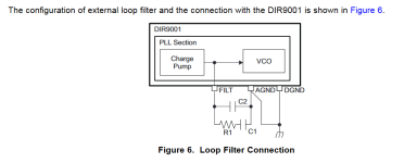
@fabrice63, arrange the connection of the PLL filter components to ground a little more, DS is quite precise here. Panasonic ECHU is a good choice for SMD film or you can freely use COG.
Separate the power supply of the DIR9001 itself from the rest. Try that DIR9001 has its own secondary on the transformer. This is the difference between an ordinary and top-quality DAC, as well as the quality of the regulator.
Separate the power supply of the DIR9001 itself from the rest. Try that DIR9001 has its own secondary on the transformer. This is the difference between an ordinary and top-quality DAC, as well as the quality of the regulator.
Attachments
Here are some hints, although most are for the DAC board and not this logic board..
-Limit input bandwith to below 10Mhz, it does not help you and increases ground bounce. We discussed it in the thread previously but here is article to help you. Actually there's more on that site, you should read all of them, in order, they're very good.
-If you do not use 50Hz reclock, DEM caps should absolutely be C0G, or film. Otherwise, low leakage like UKL's.
-Take extreme care of DEM capacitors return currents.
-Minimise loop length for all current return paths, loop inductance
-Decouple all ICs locally with smaller value ceramic cap that is close to the pin.
-The DGND should be connected only on place with the AGND pin right next to the input pins (pin 4 or 5 or something). Dont just do a whole copper pour and hope for the best, you can get good results this way also but only if your layout is good. Basically you can do two copper pours, one for digital and one for analog, and both should be connected in the area between these two pins on the DAC itself. But you must at the same time take care of DEM cap return currents, this necessitates 4 layers.
That is off the top of my head, there is more if you spend reading thread...but its enough to make a good dac for starters.
And also as grund said, do this. You can use IL715 easily, i used it when i made starting project like you now.Separate the power supply of the DIR9001 itself from the rest. Try that DIR9001 has its own secondary on the transformer. This is the difference between an ordinary and top-quality DAC, as well as the quality of the regulator.
Question about CM6631A - it has two SPDIF inputs and outputs. What is the purpose of the extra receiver? Or it can not get stream from spdif and out it to i2c dac.
38 XSPDIFO_0 DO S/PDIF transmitter Programmable 3.3V output buffer
40 XSPDIFI_0 DI S/PDIF receiver 3.3v input buffer, Schmitt trigger, pull-down
38 XSPDIFO_0 DO S/PDIF transmitter Programmable 3.3V output buffer
40 XSPDIFI_0 DI S/PDIF receiver 3.3v input buffer, Schmitt trigger, pull-down
Hi all ,
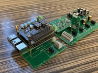
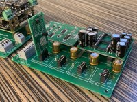
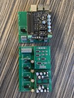
After having controled hundred times my pcb routing , I finally make them build by jlcpcb , they make a good job for the money")
I decided to populate the pcb's step by step , so here is the dir9001 section and the result is ok , next I will populate the logic section and see how it goes

the spdif source is the digital output of an cd player
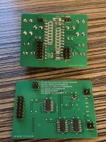
here is part of the logic view :

.
After having controled hundred times my pcb routing , I finally make them build by jlcpcb , they make a good job for the money
I decided to populate the pcb's step by step , so here is the dir9001 section and the result is ok , next I will populate the logic section and see how it goes
the spdif source is the digital output of an cd player
here is part of the logic view :
.
Last edited:
The previous picture (post 8216 ) was not good , contact issues was occuring and sample rate was off
fact is that this project , as it start at post 6116 is meant to run with left justified , for many reasons explain all along this thread , I2S as much as I understood is noisy , this setup is complex enought to bring in issues like noises and stuff
.
fact is that this project , as it start at post 6116 is meant to run with left justified , for many reasons explain all along this thread , I2S as much as I understood is noisy , this setup is complex enought to bring in issues like noises and stuff
.
Last edited:
Hi, building my dac: TDA1541a (50Hz DEM mod) with I2S to simultaneous converter. Each power supply voltage will be final regulated by Jung-Didden super regulators, these will be fed by LM317/337 pre-regulators.
I2S signal is generated by a raspberry Pi 4, a Ian Canada shieldpi pro and Fifopi Q7.
IV converter not sure yet, but tend to go with the discrete diamond of Pedja Rogic discrete.
I2S signal is generated by a raspberry Pi 4, a Ian Canada shieldpi pro and Fifopi Q7.
IV converter not sure yet, but tend to go with the discrete diamond of Pedja Rogic discrete.
Attachments
- Home
- Source & Line
- Digital Line Level
- Building the ultimate NOS DAC using TDA1541A