Ryanj implemented only John's i2s to simultaneous schematic. The signed magnitude schematic has to date only been implemented by a couple of users (and i mean like, John, koldby, and one other i think that we know of in this thread) on protoboards, and xaled made one board that was never tested until he sent it to me, but it didn't work as far as i could surmise (small schematic error but didnt work even after alteration but who knows, N = 1 here). So this is very untested and unknown territory as far as it goes.
Your comment turning attention to this is appreciated Tam Lin and is constructive, sadly, the pool of people who can even deduce this, let alone have the abilities to play with digital logic like this is fairly small in this thread, myself included...soo...we will have fun beating this horse indeed")
Your comment turning attention to this is appreciated Tam Lin and is constructive, sadly, the pool of people who can even deduce this, let alone have the abilities to play with digital logic like this is fairly small in this thread, myself included...soo...we will have fun beating this horse indeed
You cannot do a proper sign-magnitude solution with 74HC logic operating on the I2S bit stream because you have to do arithmetic on the entire sample. That is obvious it you study the PCM63 or PCM1702 datasheets.
I have no interest in the TDA dac but if I did, I would implement sign-magnitude using a foobar plugin. Coming from foobar, each sample is a unity normalized, 32-bit floating point fraction. The plugin would convert the fraction to a 16-bit integer and spawn four threads to create four variations of the sample for each channel, +plus, -plus, +minus, and –minus. Those variations would be sent to a PCB with 4 TDA1541. Each TDA would convert its samples and sum the outputs as appropriate.
I have no interest in the TDA dac but if I did, I would implement sign-magnitude using a foobar plugin. Coming from foobar, each sample is a unity normalized, 32-bit floating point fraction. The plugin would convert the fraction to a 16-bit integer and spawn four threads to create four variations of the sample for each channel, +plus, -plus, +minus, and –minus. Those variations would be sent to a PCB with 4 TDA1541. Each TDA would convert its samples and sum the outputs as appropriate.
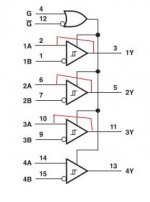
Hello!Universal I2S interface schematics
Hi all,
Problem1: SPDIF jitters
Problem2: I2S comes in different formats (compatibility)
Problem3: How to transport I2S to a external DAC
Solution: Universal Philips I2S interface (can be added to almost every transport).
Basically SPDIF jitter occurs because both data and clock signals are mixed using Biphase Mark Code and then transported to the DAC by a optical, coax or differential interface cable of a few meters, jitter is added to the integrated clock signal by the varying data content.
So let's forget about SPDIF and move on to I2S,
What signals are present in almost every transport? SPDIF and the master clock (low jitter guido tent or elso kwak clock).
Now suppose the the audio interface chip (CS8412) was placed in, or very close to the transport instead of the DAC. It could be directly driven by the SPDIF output signal of the digital processor chip without using long cables or transformers. It would also automatically convert to philips I2S format (jumper settings). Then the icing on the cake, BCK, DATA and WS can be synchronously reclocked by the (low jitter) master clock that has a fixed phase relation to both WS and BCK. D-flipflops can be used for reclocking.
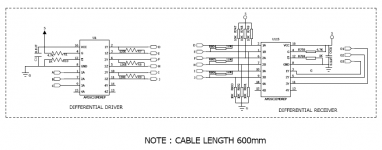
Now we have a universal very low jitter philips I2S interface in the transport. The 3 signals WS, BCK and DATA can be transported by using 3 differential RS422 interface drivers (1 X AM26LS31). On the receiving side (DAC) we use RS422 interface receivers (1 X AM26LS32), the lines can be terminated at the DAC side (54 Ohm). And why not use a standard cable available for this purpose: (screened) cat5 (4 X twisted pair) network cable. I am sure this will significantly reduce jitter as the transported clock signal is a non-modulated squarewave of a constant frequency. It will also solve I2S compatibility problems.
Oh, yes I already added a rough concept schematic diagram of this universal I2S interface. I am sure lots of improvements can be made, but it's a start.
I tried this on philips interface on my philips 620 which i use as a transport, but it doesn't work, the sound is distorted. I was wondering if pins 4 and 12 (both of 31 and 32) must be connected to 5v or PIN 4 to 5v and PIN 12 to gnd as in the attached photo.
Attachments
No try to enable it like in the datasheets.
https://www.quick-teck.co.uk/Management/EEUploadFile/1469530629.pdf
All G to Vcc 5V and all -G disconnect
or another way, All G leave unconnected and all -G connect to ground.
.
This option of enabling can be usefull for selecting lines
I did it with simple inverter.
Also find that sound was better even with shorter lines inside the dac... Dont know how to explain...
I think i used same drv/rcv pair but termination was little different not hard with 50ohms.
.
try to get first standard enabling
after that measure with scope diff lines and find better termination values of reistors?
Sorry but I could not understand.No try to enable it like in the datasheets.
https://www.quick-teck.co.uk/Management/EEUploadFile/1469530629.pdf
All G to Vcc 5V and all -G disconnect
or another way, All G leave unconnected and all -G connect to ground.
.
This option of enabling can be usefull for selecting lines
I did it with simple inverter.
Also find that sound was better even with shorter lines inside the dac... Dont know how to explain...
I think i used same drv/rcv pair but termination was little different not hard with 50ohms.
.
try to get first standard enabling
after that measure with scope diff lines and find better termination values of resistors
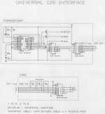
I need to connect my cd transport to my tube dac with tda1541.
Both are connected via rj45 connections and LAN cable.
I used chip 31 on transport and chip 32 on dac but they don't talk.
Bypassing AM26LS32 and lifting the 56 ohm resistors instead it also works with AM26LS31 (with pins4 and 12 connected to 5v).
Strange!
Could you help me solve my problem?
Attachments
Last edited:
OR If it is on this place receiver
You bypassed like this
BUT that will be little strange because of the serialresistor only at one leg...
.
Try to find with the scope what are all signals present at the cable connector after the driver
.
You bypassed like this
BUT that will be little strange because of the serialresistor only at one leg...
.
Try to find with the scope what are all signals present at the cable connector after the driver
.
Attachments
Problem solved, - lrck inverted with - data on 31 chip driver .OR If it is on this place receiver
You bypassed like this
BUT that will be little strange because of the serialresistor only at one leg...
.
Try to find with the scope what are all signals present at the cable connector after the driver
.
Now is working fine
Thanks for your advices.
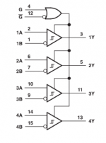
In this diagram the PIN out of AM26LS32 are wrong.Universal I2S interface schematics
Hi all,
Problem1: SPDIF jitters
Problem2: I2S comes in different formats (compatibility)
Problem3: How to transport I2S to a external DAC
Solution: Universal Philips I2S interface (can be added to almost every transport).
Basically SPDIF jitter occurs because both data and clock signals are mixed using Biphase Mark Code and then transported to the DAC by a optical, coax or differential interface cable of a few meters, jitter is added to the integrated clock signal by the varying data content.
So let's forget about SPDIF and move on to I2S,
What signals are present in almost every transport? SPDIF and the master clock (low jitter guido tent or elso kwak clock).
Now suppose the the audio interface chip (CS8412) was placed in, or very close to the transport instead of the DAC. It could be directly driven by the SPDIF output signal of the digital processor chip without using long cables or transformers. It would also automatically convert to philips I2S format (jumper settings). Then the icing on the cake, BCK, DATA and WS can be synchronously reclocked by the (low jitter) master clock that has a fixed phase relation to both WS and BCK. D-flipflops can be used for reclocking.
Now we have a universal very low jitter philips I2S interface in the transport. The 3 signals WS, BCK and DATA can be transported by using 3 differential RS422 interface drivers (1 X AM26LS31). On the receiving side (DAC) we use RS422 interface receivers (1 X AM26LS32), the lines can be terminated at the DAC side (54 Ohm). And why not use a standard cable available for this purpose: (screened) cat5 (4 X twisted pair) network cable. I am sure this will significantly reduce jitter as the transported clock signal is a non-modulated squarewave of a constant frequency. It will also solve I2S compatibility problems.
Oh, yes I already added a rough concept schematic diagram of this universal I2S interface. I am sure lots of improvements can be made, but it's a start.
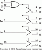
The correct PIN out are:
1Y= 3
2Y= 5
3Y= 11
4Y= 13
PIN 12 of AM26LS32 and AM26LS31 must be float, only PIN 4 must be connect to 5V
Attachments
Since this is his thread and most people are interested in how his quest is going... why spoil the fun?The point is that this thread is about tda1541a. It is not a thread about John's latest product for sale. That should be in a commercial section.
I for one totally agree.Since this is his thread and most people are interested in how his quest is going... why spoil the fun?
NahThe point is that this thread is about tda1541a. It is not a thread about John's latest product for sale. That should be in a commercial section.
this thread is about johns work
Well, you might as well ask about his latest work because i feel pretty much momentum of thread is concluded, tda interest seems a bit died down, i think (but dont quote me on this) John mentioned he moved on to other things and got out of tda1541 what he wanted...now he just anwsers questions here and there out of generosity and good nature it seems. And questions bump the thread up anyway so it has its positive aspect..
Report from me: I have in front of me currently latest (v3) redesign of signed magnitude PCB, xaled's version of just i2s to signed magnitude logic, and testing this with my JLsounds and xaled's Amanero, together with logic analyzer (i still have to return this stuff to him!). Sadly, though i have implemented about a dozen different dacs at this point, this one is a horse that refuses to be broken. Yes regular i2s and simultaneous work, and yes you can use two tda's and double the currents and all that, but that isn't breaking new ground.
Currently in life i am also very busy and in times of change, so i kind of doubt there will be a v4 if i dont get this to work in a few days. Embarassingly, easily well over 100hrs into this project just reading, researching, designing, revisioning...and that is with all the "blueprints" basically already provided by John...
I plan to send out board to some standing and/or interested thread participants upon request, to mess around with it themselves if they want to, as it should be all correct in theory...
Anyway, more from me later.
P.S i am zbunjen from this thread, just forum name change
Dear John has long ago attained the State of Grace so He is not bounded by earthlings' laws, rules, norms and statutes that are imposed (or self/imposed) on us...It must be the ultimate NOS DAC using TDA1541a, right?
I Love You All, Oh so much...
M.
- Home
- Source & Line
- Digital Line Level
- Building the ultimate NOS DAC using TDA1541A