Higher sample rates require higher clock and data rates in source, interlink and DAC circuits. Circuits are never perfect, the major issues with digital audio are stray capacitances and stray inductances in source, interlink and DAC. The combination of high frequency clock and data rates with these parasitics will cause major issues with digital audio that are still not fixed. One of the results is source dependency (every bit-perfect source still sounds different). When clearly audible source dependency occurs, digital audio is still far from optimal.
Every imaginable interference that is added to the always present digital audio related signals will make matters worse, think of (RF) ground loop noise and power supply (mains) noise. All data and frequency signals will crosstalk and create one big unpredictable interference spectrum that can reach into the GHz range (harmonics). Even Bluetooth, GSM and WIFI add to this mix. This complex and constantly varying large bandwidth spectrum will be de-modulated by P-N junctions for example (think of radio receivers). Then demodulation products can be formed from two or more inaudible frequencies that will now fall within the audio spectrum (same happens with radio, television and wireless phones, but here this is desired to get the information across).
This interference cannot be blocked by 20KHz brickwall filters because these frequencies fall within the audio spectrum itself. The result is audible degrading / change of sound even when using world's best synchronous re-clockers in a DAC.
Hi
Sorry to ask a question about this quite old post, but a friend of mine asked be about it.
Do you have any measurement about all your affirmations?
Kind regards
Thierry
No, but also TDA1541A is not a thing you implement when SINAD is your priority, kind of thingHi
Sorry to ask a question about this quite old post, but a friend of mine asked be about it.
Do you have any measurement about all your affirmations?
Kind regards
Thierry
")
That being said it measures respectably, see post 7250
HiNo, but also TDA1541A is not a thing you implement when SINAD is your priority, kind of thing
That being said it measures respectably, see post 7250
Thanks for your answer.
I was not speaking about SINAD😉
But, for example, about GSM/Wifi/BT interferences demodulation falling in the audio spectrum that should be measurable, using of course well shielded « interlinks » as named by @ecdesigns to avoid any antenna effects.
Best and kind regards.
Thierry
My bad, you're right i interpreted it wrong.Hi
Thanks for your answer.
I was not speaking about SINAD😉
But, for example, about GSM/Wifi/BT interferences demodulation falling in the audio spectrum that should be measurable, using of course well shielded « interlinks » as named by @ecdesigns to avoid any antenna effects.
Best and kind regards.
Thierry
It is what happens when come home sit on diyaudio after some rakija
Still, i can tell you from reading this thread for many hours i have not come across what you seek, but godspeed, it would not be first time i missed something
Finally caught some time so hooked up @xaled 's board.
Taking it slowly and double checking everything, looking at pcb, seeing what's what etc.
First looked with logic analyser, everything seems ok.
I connect it up, eureka, we have sine wave...or not so fast
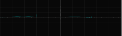
There is digital buzz sound, i mess around with everything, switching between dacs, but when a setting is not correct it is immediately noticable, and the setting that should be correct is indeed something close to a sine, but with some square wave overtones.
We are playing a pure sine wave, so the signal should remain constant. But look at the data line (purple).

The data lines are fairly "jittery" and change their pulse widths all the time. Since the signal is a constant sine, the data lines should be constant too, right? Well, this was a red herring for me because my working simultanous mode Jlsounds board has a similar jittery data line behaviour but sounds just fine. 100 megasamples per second on the logic analyzer, so i dont know if its to blame.
DAC IC uses one channel for positive, other for negative half wave, so the two must follow one after the other carefully. Connecting DOR+ and DOR- would be this, but how about connecting DOR+ and IDOR+ for example (i.e inverted version of same signal)?
Well, now they should perfectly cancel out, it will clock in same but inverted signal in both channels at the same time, output the signal, they should cancel and silence should be the answer, right? But actually what we get is something similar to the distortion that is present when normal listening.

There is an exact 20 nanosecon delay between the line and its inverted counterpart, ok, this is due to logic speed. I am not sure if this sort of precision will matter for clocking in I2S.
But assuming it matters, and so it will not combine correctly, i.e due to timing mismatch the other does not "hand off" the signal at the right time. So it would look something like crossover distortion.

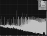
Here is with the correct setting of the signals. Indeed we can see it, and it also seems to be worst at same side of the sine, because the error is consistent.
Here is with taking same signal but inverted (DOR- and IDOR-).

We are left with only the error itself (this is quite audible)
Only top halfwave

Only bottom halfwave

After some digging @Hans Polak already commented on this in post 7206 how timing difference would present itself in spectra.

We have something like

Now would be a question, is this inherent with the schematic, or just xaled's implementation (cant find post now for some reason).
Is this the half bit delay error that was fixed in 7092?
@koldby i think you're one of the only people who had hands on experience with this sort of headache.
Last option is, this is just expected behaviour for untrimmed, just simple summing style and TDA1541A will require mandatory trimming if you plan to use signed magnitude?
Taking it slowly and double checking everything, looking at pcb, seeing what's what etc.
First looked with logic analyser, everything seems ok.
I connect it up, eureka, we have sine wave...or not so fast
There is digital buzz sound, i mess around with everything, switching between dacs, but when a setting is not correct it is immediately noticable, and the setting that should be correct is indeed something close to a sine, but with some square wave overtones.
We are playing a pure sine wave, so the signal should remain constant. But look at the data line (purple).
The data lines are fairly "jittery" and change their pulse widths all the time. Since the signal is a constant sine, the data lines should be constant too, right? Well, this was a red herring for me because my working simultanous mode Jlsounds board has a similar jittery data line behaviour but sounds just fine. 100 megasamples per second on the logic analyzer, so i dont know if its to blame.
DAC IC uses one channel for positive, other for negative half wave, so the two must follow one after the other carefully. Connecting DOR+ and DOR- would be this, but how about connecting DOR+ and IDOR+ for example (i.e inverted version of same signal)?
Well, now they should perfectly cancel out, it will clock in same but inverted signal in both channels at the same time, output the signal, they should cancel and silence should be the answer, right? But actually what we get is something similar to the distortion that is present when normal listening.
There is an exact 20 nanosecon delay between the line and its inverted counterpart, ok, this is due to logic speed. I am not sure if this sort of precision will matter for clocking in I2S.
But assuming it matters, and so it will not combine correctly, i.e due to timing mismatch the other does not "hand off" the signal at the right time. So it would look something like crossover distortion.
Here is with the correct setting of the signals. Indeed we can see it, and it also seems to be worst at same side of the sine, because the error is consistent.
Here is with taking same signal but inverted (DOR- and IDOR-).
We are left with only the error itself (this is quite audible)
Only top halfwave
Only bottom halfwave
After some digging @Hans Polak already commented on this in post 7206 how timing difference would present itself in spectra.
We have something like
Now would be a question, is this inherent with the schematic, or just xaled's implementation (cant find post now for some reason).
Is this the half bit delay error that was fixed in 7092?
@koldby i think you're one of the only people who had hands on experience with this sort of headache.
Last option is, this is just expected behaviour for untrimmed, just simple summing style and TDA1541A will require mandatory trimming if you plan to use signed magnitude?
Attachments

Last edited:
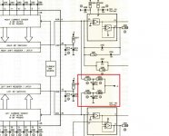
Think there might have been a mistake in the sch used for making xaled's board, notice U2B.

It was inverted in the fix, since original sch was made for left justified, and data was not clocking in correctly, but here its still non-inverted. Also smart use of complementary output of U1A to eliminate one inverter (also U1A in John's).
John's revised sch in 7092, look at U7:

It was inverted in the fix, since original sch was made for left justified, and data was not clocking in correctly, but here its still non-inverted. Also smart use of complementary output of U1A to eliminate one inverter (also U1A in John's).
John's revised sch in 7092, look at U7:
I used to have wav files with bit patterns generated by a python script from the internet. I adjusted the script a bit and could generate 16 bit patterns like all 1s or all 0s or all 1s except for LSB or MSB etc. This was useful to debug the logic.
Now I only need to found the script and the files. Will update you once I found it.
You could also look in parallel if could could fine one.
Now I only need to found the script and the files. Will update you once I found it.
You could also look in parallel if could could fine one.
Here is my original schematic from 2019,
Based on this schematic, connection to U2B pin 9 must be moved to U2B pin 8.
U2B corresponds with U7 in my schematic.
74LVC1G80 = Flip-Flop with inverted Q output.
74LVC1G79 = Flip-Flop with non-inverted Q output.
You could lift pin 9 (U2B) and use a wire to connect U2B pin 8 to U16 pin 1. This way you don't have to cut traces.
hello John,
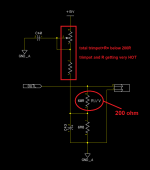
i tried to changed the IV resistor into 200R to get more gain.
i still can trim into zero dc out, sound is normal, and with more gain.
but the trimpot and parallel resistor become very hot.
how to get rid from this hot?
thanks.
Peter
so now i reduce the voltage into 5v dc.
heat are normal (warm), still i can trim into zero volt and steady.
i don't have measurement devices so i don't know about the distortion,
but to my ear, giving 5v in IV stage is sounding better than 15v.

Hi For +15V Io at the 200ohm total R (pot +R) is 15V/200ohm=0.075A cca. That is 0.075Ax15V=1.125W of power dissipation.
I You want to get just warm these elements You have to increase power of elements to 4X of calculated dissipation so that total R should be from 4-5W...
Make this fixed R to be main final value close to 200ohms some standard 180ohm value or 4x750ohm/1W in parallel to get 187.5 ohm/4W
and pot value from 47 ohms. In this way dissipation will happens at the 4W R mainly and pot wil not be affected much.
Zdravo Zoran,Is there any progress about lifting wrong pin and connecting to proper?
I lifted the pin on the SOIC, and then bridged the pad over to the adjecent pin with solder (since inverted output is pin 8, and this is pin 9). I triple checked in sheet these pins and orientation and everything to validate everything physically is as should be schematically, and tested continuity with multimeter.
I thought it would finally be the ticket, but what happens is nothing. Logic analyser shows outputs as expected, but for some reason TDA's only produce silence and cannot decode this. I cannot explain it at all, before at least we had noises. This is why i triple checked everything with continuity meter. If you revert it back it will play these noises with extremely high harmonics again, and simultanous mode plays perfectly, so not like the dac's pooped out.
Of course i also tried all possible permutations on my board, studied schematic over and over, measured everything, but no.
It was a dissapointing development to report so i didnt say anything thinking maybe solution comes to me in a dream, but it did not.
Anyway, this is getting frankly dizzying and i want to come to some conclusion of this so i can at least send xaled the package back + board.
So i will redesign digital side with 74lvc74 like xaled did, except with this pin corrected to match up to ecdesigns (in other words, this pin lift will be incorporated into design already), in any case it should be equivalent to ecdesigns design, just using 74-74 logic. It will either work (according to logic) or will produce silence (according to how much misfortune i have with this). In meantime i did some other improvement to analog design side of the board, and also some minor things that i noticed while using the v1 that of course, you only notice once you have it in your hand.
Also, it is summer, so during some parts of it i will not be in my house where the boxes of components to build these are, in addition working a job, writing masters degree thesis, and design board for 3 other projects in parallel, it slows development.
Hello, yes, i tried first the * , double checking according to the diagram, and making sure xaled board's wiring is according (other than the pin lift thing which was corrected). I also confirmed with logic analyser these complementary outputs are indeed complementary, other than the 20 nanosecond delay due to 50mhz logic speed of HC series, i will try with LVC after making new batch of boards, although i vaguely remember John mentioned long ago the faster logic is not necessary. (later i also tried the non * outputs, i tried basically all permutations i could think of)But now I am with ECdesign IBS PDF...
For minimum working mode You need 2 TDA1541A dacs.
Take a look at the "*" marked outputs please.
Each dac chip operate for one channel only.
...
Did You checked proposed DAC chips connections?
So one TDA1541 chip received for example DOR- / DOR+ on pins 3 and 4, while running in simultaneous mode (-5v to pin 27). I can confirm this works with normal simultaneous mode signal . Although with of course making sure it has the correct I/V, since it does not operate under same principles. In simultaneous with 2x dac chips i implemented as parallel, but signed magnitude each dac chip (containing two dacs) forms one channel, by having its outputs summed together, containing each half-wave. (sorry if i worded this badly)
I will just note again for transparency, i used two non-A versions of TDA1541, but as far as i understood the input logic for them is the same, i did not see difference here in the data sheets so it should not be the difference.
It's amusing to see a new-found interest in sign-magnitude DACs. Too bad no one bothers to learn about the process but just copies the first schematic that comes along. The ecdesigns circuit has many problems. The output is not monotonic. Every sample has a +/- 1/2 LSB offset added. Every positive sample has an additional -1 LSB offset added. It adds 16 chips that consume power and add noise. Have fun.Here is my original schematic from 2019,
- Home
- Source & Line
- Digital Line Level
- Building the ultimate NOS DAC using TDA1541A