Your Latest I2S Atteunator
Hi John,
Thank you for your reply.
See attachment. Is my understanding correct.
Hi Audiohifi,
Circuit lay-out is -very- critical, one would have to place the complete circuit (especially the DEM clock circuit) over a solid ground plane and use shortest possible wiring (millimeters) and effective decoupling. Failing to do so causes instabilities (noise).
I now use a free running low jitter DEM oscillator:
470pF film cap between pin 16 & 17.
6K8 resistor between pin 15 & 16.
6K8 resistor between pin 15 & 17.
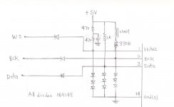
The latest I2S attenuators I used were diode attenuators:
Diode #1, cathode to I2S source, anode to TDA1541A I2S input.
Diode #2 … #4 in series, cathode to ground, anode to TDA1541A I2S input.
Pull up resistor, 1K for WS and DATA, 330R for BCK between +5V and TDA1541A I2S input.
1N4148 diodes will do fine. One could also use an IR led (1V2) with a diode in series to replace the 3 diode diodes in series. Impedance would be a bit lower this way.
These diode attenuators produce a very clean 1V2pp I2S signal that varies between 0V6 and 1V8.
The pull-up resistors may pollute the 5V power supply. One could use split pull-up resistors (470R, 470R for example) and decouple the junction to GND using a capacitor.
Hi John,
Thank you for your reply.
See attachment. Is my understanding correct.
It was not easy but I managed to convert I2S 64 bits / frame (44.1/16) two’s complement into offset binary, 16 bit data bursts for TDA1541A in simultaneous mode.
5 bits counter plus decoder was used for clock stopping, discriminating the MSB “on the fly” to invert MSB only in the serial data stream (two’s complement to offset binary conversion) and to generate a LE pulse just before MSB.
/O0, Q1, Q2, Q3, and Q4 enter a NOR gate creating the MSB discrimination pulse.
O0, Q1, Q2, Q3, and Q4 enter a NOR gate creating the LE pulse.
WS, and Q4 enter a NOR gate for creating the BCK enable pulse.
The counter is clocked by BCK and reset with a one shot triggered by WS (synchronisation between conter and WS).
In order to complete the circuit I would need either a 32 bit delay circuit to align both L and R channels (simultaneous mode stereo), or a dual mono converter (simultaneous mode in dual mono).
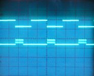
Attached oscillogram shows the stopped clock BCK signal. Upper trace shows the WS signal, lower trace shows the periodic bit clock bursts (2.8224 MHz), each contains 16 BCK pulses.
The whole point of this exercise is to obtain longest possibe period of silence (absence of I2S interference in the TDA1541A and attached circuits) during each sample period.
I2S stream now looks as follows, LE pulse is generated, lasting one BCK clock cycle. 16 bits of data are clocked in simultaneously. Then the I2S stream is shut down completely (WS, DATA and BCK shut down for 75% of the sample period).
The created silence (absence of switching noise) has positive impact on sound quality.
5 bits counter plus decoder was used for clock stopping, discriminating the MSB “on the fly” to invert MSB only in the serial data stream (two’s complement to offset binary conversion) and to generate a LE pulse just before MSB.
/O0, Q1, Q2, Q3, and Q4 enter a NOR gate creating the MSB discrimination pulse.
O0, Q1, Q2, Q3, and Q4 enter a NOR gate creating the LE pulse.
WS, and Q4 enter a NOR gate for creating the BCK enable pulse.
The counter is clocked by BCK and reset with a one shot triggered by WS (synchronisation between conter and WS).
In order to complete the circuit I would need either a 32 bit delay circuit to align both L and R channels (simultaneous mode stereo), or a dual mono converter (simultaneous mode in dual mono).
Attached oscillogram shows the stopped clock BCK signal. Upper trace shows the WS signal, lower trace shows the periodic bit clock bursts (2.8224 MHz), each contains 16 BCK pulses.
The whole point of this exercise is to obtain longest possibe period of silence (absence of I2S interference in the TDA1541A and attached circuits) during each sample period.
I2S stream now looks as follows, LE pulse is generated, lasting one BCK clock cycle. 16 bits of data are clocked in simultaneously. Then the I2S stream is shut down completely (WS, DATA and BCK shut down for 75% of the sample period).
The created silence (absence of switching noise) has positive impact on sound quality.
Attachments
Latest I2S Atteunator
Hi John,
My earlier sketch of the schematic is wrong.
Please check this one and comment.
Thank You
Hi John,
Thank you for your reply.
See attachment. Is my understanding correct.
Hi John,
My earlier sketch of the schematic is wrong.
Please check this one and comment.
Thank You
Attachments
Hi Audiohifi,
It’s correct but use same split pull-up desistor with decoupling cap on BCK and DATA as well.
So you need 6 resistors and 3 decoupling caps in total.
Remove the 10mH choke, it causes ringing, emits EMI / picks up EMI. Two resistors with a decoupling cap will do fine.
See attachment. Is my understanding correct.
It’s correct but use same split pull-up desistor with decoupling cap on BCK and DATA as well.
So you need 6 resistors and 3 decoupling caps in total.
Remove the 10mH choke, it causes ringing, emits EMI / picks up EMI. Two resistors with a decoupling cap will do fine.
Latest I2S Atteunator
Thanks for the reply.
Your explanation is refering to the schematics shown below right?
Hi John,Hi Audiohifi,
It’s correct but use same split pull-up desistor with decoupling cap on BCK and DATA as well.
So you need 6 resistors and 3 decoupling caps in total.
Remove the 10mH choke, it causes ringing, emits EMI / picks up EMI. Two resistors with a decoupling cap will do fine.
Thanks for the reply.
Your explanation is refering to the schematics shown below right?
Attachments

Last edited:
The pull-up resistors may pollute the 5V power supply. One could use split pull-up resistors (470R, 470R for example) and decouple the junction to GND using a capacitor.
Please help with advice on value and type of decoupling cap?
Thank you, marco
Hi there,
Sorry if I am spamming but as a novice I read a lot from this thread and became a fan of TDA 1541. Since I am not able to produce the DAC myself I have bought one and now trying to upgrade it. Will you please suggest may I utilize this for some initial improvement -
The DEM oscillator is the free running low jitter version:
- 470pF between pins 16 & 17.
- 6K8 between pins 15 & 16.
- 6K8 between pins 15 & 17.
The part of the schematics is attached.
Thanks in advance,
Ignat
Hi niamex,
Your schematics indicate the TDA1541, not the TDA1541A.
TDA1541 has built-in DEM oscillator timing cap. Philips engineers integrated the timing cap in the TDA1541 in an attempt to reduce problems with deterministic DEM oscillator jitter.
This means that pins 16 and 17 of the TDA1541 are no longer connected to the DEM oscillator circuit (datasheet indicates n.c.).
So this low jitter DEM oscillator mod can’t be used with the TDA1540. It only works with the TDA1541A.
Will you please suggest may I utilize this for some initial improvement
Your schematics indicate the TDA1541, not the TDA1541A.
TDA1541 has built-in DEM oscillator timing cap. Philips engineers integrated the timing cap in the TDA1541 in an attempt to reduce problems with deterministic DEM oscillator jitter.
This means that pins 16 and 17 of the TDA1541 are no longer connected to the DEM oscillator circuit (datasheet indicates n.c.).
So this low jitter DEM oscillator mod can’t be used with the TDA1540. It only works with the TDA1541A.
Your schematics indicate the TDA1541, not the TDA1541A.
Hi ECDESINS,
Thanks for your prompt reply. Sorry - schematics is mistaken by the designer and I have copied and pasted without watching. IT IS 1541 A - otherwise I wouldn't ask you. You can see the cap 471 pf there. So I understand I can go for the little mod ? Forgive my ignorance -/I am just a lawyer/ but it could be interesting for the friends here that I am prepared to try 12 electrolytic decoupling caps of 1 uf plus 2 of 2.2 uf for the MSB - directly on the chip legs from the bottom /positive to ground/MAL212855228E3 - CAP, ALU ELEC/. All bypassed on the top 0.1 uf.
Will inform results when ready - soon.
Appreciating your attention,
Thanks,
Ignat
Hi John, hi everybody
(AWESOME new products John! I am especially thrilled by the reactor circuit)
This was not under typical listening conditions. I heard the left channel distortion when listening late at night (low background noise) AND using digital volume. As you know, digital attenuation is not a good thing as you will be losing bits of resolution and the problems of digital will be exacerbated.
Thinking about it now, digital volume is a *bad* idea, worse possible situation, as you get no attenuation whatsoever of the glitches and noise that inevitably come along with your converted audio.
Back then, using only AOR solved it for me, however I am about to try the left channels again, either in parallel or differential.
This difference between AOL and AOR has shown up in measurements as well (from Stereophile):
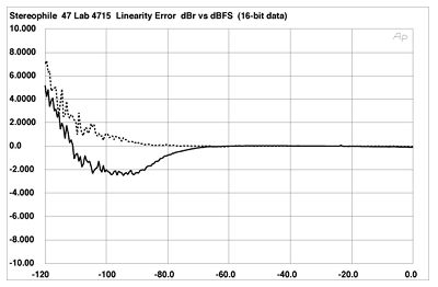
Fig.7 47 Laboratory 4715, departure from linearity, 16-bit data (2dB/vertical div., right channel dashed).
-Alex
(AWESOME new products John! I am especially thrilled by the reactor circuit)
I´ve been quoted, let me explain this left channel thing (TDA1543).it seems according some forums that the left channel has higher distortion and less resolution than the right channel
This was not under typical listening conditions. I heard the left channel distortion when listening late at night (low background noise) AND using digital volume. As you know, digital attenuation is not a good thing as you will be losing bits of resolution and the problems of digital will be exacerbated.
Thinking about it now, digital volume is a *bad* idea, worse possible situation, as you get no attenuation whatsoever of the glitches and noise that inevitably come along with your converted audio.
Back then, using only AOR solved it for me, however I am about to try the left channels again, either in parallel or differential.
This difference between AOL and AOR has shown up in measurements as well (from Stereophile):
Fig.7 47 Laboratory 4715, departure from linearity, 16-bit data (2dB/vertical div., right channel dashed).
-Alex
Last edited:
Hi wlowes,
Low amplitude ac voltage will be generated across the I/V resistor. So it would be best to place it as close to the amplifier input as possible. The CCS in the TDA1541A should keep the current to the I/V resistor constant, so longer wiring here would be less problematic. However make sure that these wires don't pick up EMI (use suitable screening).
When using a simple resistor for I/V, does the physical placement of the resistor matter? Should it be close to the pins of the TDA1541A or is it ok to put it close to the output stage?
Low amplitude ac voltage will be generated across the I/V resistor. So it would be best to place it as close to the amplifier input as possible. The CCS in the TDA1541A should keep the current to the I/V resistor constant, so longer wiring here would be less problematic. However make sure that these wires don't pick up EMI (use suitable screening).
Hi niamex,
Yes, you only have to add two 6K8 resistors to the existing timing cap of 470pF. This will greatly reduce the high level of deterministic jitter on the DEM oscillator as soon as audio data is sent to the TDA1541A.
Electrolytic caps have a DC leakage current that’s much higher compared to the 61nA LSB current. So using electrolytic caps is not a good idea.
Paralleling caps should be done with caution as resonance effects may occur between the paralleled caps. This could lead to poor decoupling. So it’s best to thoroughly test and measure the effects of paralleling caps.
Possible reason for the impact of active divider filter cap properties on sound is the high level of deterministic jitter on the DEM oscillator when using the Philips datasheet application (modulated carrier frequency).
Philips engineers were well aware of this issue, in an attempt to fix it they integrated the timing cap in the TDA1541 but this didn’t fix the problem. So it was placed externally again with the TDA1541A.
So I understand I can go for the little mod
Yes, you only have to add two 6K8 resistors to the existing timing cap of 470pF. This will greatly reduce the high level of deterministic jitter on the DEM oscillator as soon as audio data is sent to the TDA1541A.
I am prepared to try 12 electrolytic decoupling caps of 1 uf plus 2 of 2.2 uf for the MSB
Electrolytic caps have a DC leakage current that’s much higher compared to the 61nA LSB current. So using electrolytic caps is not a good idea.
Paralleling caps should be done with caution as resonance effects may occur between the paralleled caps. This could lead to poor decoupling. So it’s best to thoroughly test and measure the effects of paralleling caps.
Possible reason for the impact of active divider filter cap properties on sound is the high level of deterministic jitter on the DEM oscillator when using the Philips datasheet application (modulated carrier frequency).
Philips engineers were well aware of this issue, in an attempt to fix it they integrated the timing cap in the TDA1541 but this didn’t fix the problem. So it was placed externally again with the TDA1541A.
Hi Alexandre,
We just completed the TDA1541A-based SD2-player prototype (attached pictures).
It runs on two external power supplies, 12V supply for the SD-transport and a 24V supply for TDA1541A, masterclock and output stage.
Stepped shunt volume control is included and output signal equals 4Vpp. An AUX input is also provided.
The USB to RS232 converter chip is now built in so the SD2-player can be directly connected to a computer using a mini USB connector.
It runs on the existing SD-player computer application.
I used selected TDA1543 chips only, these have similar low distortion, full-scale current and DC-offset on both channels. From 100 TDA1543 chips, approx. 25 had good matching, 5 were excellent.
I also made sure TDA1543 output compliance of 50mVpp was met, failing to do so can also lead to different distortion between both channels.
With the dual mono TDA1543 test setup I used an I/V converter that ensures less than 50uVpp on the TDA1543 outputs. The lower the ac voltage on the TDA1543 outputs, the lower the distortion introduced by variable bias current source, bit switches, passive dividers and reference current source.
(AWESOME new products John! I am especially thrilled by the reactor circuit)
We just completed the TDA1541A-based SD2-player prototype (attached pictures).
It runs on two external power supplies, 12V supply for the SD-transport and a 24V supply for TDA1541A, masterclock and output stage.
Stepped shunt volume control is included and output signal equals 4Vpp. An AUX input is also provided.
The USB to RS232 converter chip is now built in so the SD2-player can be directly connected to a computer using a mini USB connector.
It runs on the existing SD-player computer application.
Back then, using only AOR solved it for me, however I am about to try the left channels again, either in parallel or differential.
I used selected TDA1543 chips only, these have similar low distortion, full-scale current and DC-offset on both channels. From 100 TDA1543 chips, approx. 25 had good matching, 5 were excellent.
I also made sure TDA1543 output compliance of 50mVpp was met, failing to do so can also lead to different distortion between both channels.
With the dual mono TDA1543 test setup I used an I/V converter that ensures less than 50uVpp on the TDA1543 outputs. The lower the ac voltage on the TDA1543 outputs, the lower the distortion introduced by variable bias current source, bit switches, passive dividers and reference current source.
Attachments
John, that´s an impressive low impedance I/V - 0.05 ohms!
I totally agree that chip selection makes a BIG difference with tda1543.
Point is, passive I/V can be rather ok on the right channel, the same cannot be said for the left - it´s a trend. I have 16 chips from different sources (ebay, swap meet, local) and no, it is not my implementation.
Still love the TDA1543 chip though")
I totally agree that chip selection makes a BIG difference with tda1543.
Point is, passive I/V can be rather ok on the right channel, the same cannot be said for the left - it´s a trend. I have 16 chips from different sources (ebay, swap meet, local) and no, it is not my implementation.
Still love the TDA1543 chip though
Hi niamex,
Hi ECDESIGNS,
Thanks for your comment. Will follow the suggestions and ask some guy to measure the resulting output accordingly/unfortunately I am not able to do that personally/. The electrolitics are highly recommended as Black Gates similarity ?? /the only ones/ Will try anyway and replace in case of poor results.
Thanks a lot,
Ignat
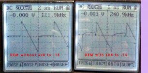
DEM with and without 6k8 to -15V
Just thought i might share some oscilloscope shots i took last night.
DEM with and without the 6k8 resistors to -15V.
They were taken from different chips running at slightly different speeds but I think this shouldn't affect the shape of the waveform.
Just thought i might share some oscilloscope shots i took last night.
DEM with and without the 6k8 resistors to -15V.
They were taken from different chips running at slightly different speeds but I think this shouldn't affect the shape of the waveform.
Attachments
DEM deterministic jitter
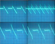
Hi ryanj’
Were these made while the TDA1541A was playing music or without audio signal? this makes a big difference. While music is playing, very high level of deterministic jitter is added to the DEM clock signal
I attached an oscillogram I just made with a professional Philips / Fluke analogue scope. Analogue scopes offer almost infinite screen resolution, digital scope screen resolution is very limited and there is the A/D conversion process plus losses.
Upper oscillograms show a circuit with only 470pF timing cap without audio (left) and with audio (right). The deterministic jitter levels are so high that the scope can no longer trigger.
Lower oscillogram shows exactly the same circuit, few minutes later, only with two 6K8 resistors soldered in.
Lower left oscillogram without music playing lower right oscillogram with music playing. Also notice the reduced switching noise levels on the low jitter DEM clock.
Hi ryanj’
Just thought i might share some oscilloscope shots i took last night.
Were these made while the TDA1541A was playing music or without audio signal? this makes a big difference. While music is playing, very high level of deterministic jitter is added to the DEM clock signal
I attached an oscillogram I just made with a professional Philips / Fluke analogue scope. Analogue scopes offer almost infinite screen resolution, digital scope screen resolution is very limited and there is the A/D conversion process plus losses.
Upper oscillograms show a circuit with only 470pF timing cap without audio (left) and with audio (right). The deterministic jitter levels are so high that the scope can no longer trigger.
Lower oscillogram shows exactly the same circuit, few minutes later, only with two 6K8 resistors soldered in.
Lower left oscillogram without music playing lower right oscillogram with music playing. Also notice the reduced switching noise levels on the low jitter DEM clock.
Attachments
- Home
- Source & Line
- Digital Line Level
- Building the ultimate NOS DAC using TDA1541A