Hi Sven257,
The dual mono circuit was tested with the TDA1543 in order to increase full scale current. This in turn was required to increase output signal amplitude while maintaining same I/V resistor value and improve bit switching characteristics.
The idea was using this circuit in a new version of the SD1-player.
However, we finally decided to use the TDA1541A instead.
Both, UD2 DAC and the new SD2-player will be based on the TDA1541A and the reactor circuit.
Both projects will fit in a similar 12mm high housing (attached pictures show the already completed UD2 DAC).
Hi John,
") nice to see you again here,
nice to see you again here,Seiing the photographs : no RCA outputs ? Is it a headphones Dac ? Jut see a 3.5 mm plug for portative headphones ?! I'm not understand if the new S1 player will be a standalone device;
On your player what will you have : SD Card reader and also RJ45 for network librairy ? USB for attached storage ?
What difference between the Reactor and the simultaneous mode used by Audial on the S player. Are you slavering the I2S output of the USB async with a masterclock which also manage the DEM clock ?
elswhere we are trying to do without unpretentious a little I2S input pcb (non commercial) for the TDA1541 with uf.l connectors for DIY and vias for analog outputs. It's a collaborative project with the good willed fellows who share their free time. I don't know the direction but do we have your permission if DEM clock and I2S attenuattor will be used ? Heard the attenuator is better without the shunt caps also...
Many questions John and some OT, sorry but I prefer concentrate for not polluting too much
Originally Posted by -ecdesigns-
I tested a TDA1543 single, two paralleled and dual mono configuration side by side. The dual mono configuration provides best perceived sound that comes closest to that of an optimised TDA1541A circuit. So the I2S splitter clearly offers advantages here.
Hi John,
So wouldn't the 'I2S splitter dual mono configuration' benefit the 1541A as well??
Last edited:
Hi Eldam,
The device on the picture is the UD2, a TDA1541A-based asynchronous USB DAC.
Connections (photo of rear view of the device):
- Mini USB connection for streaming audio on the left.
- DC socket for the external 24V supply (TDA1541A) in the center.
- 3.5mm Jack socket for audio output (4Vpp).
The new SD2-player has following connections:
- Mini USB for computer-based remote control (not for streaming!).
- DC socket for the external 24V supply (TDA1541A).
- DC socket for the external 12V supply (SD-transport).
- 3.5mm Jack socket for audio output (4Vpp).
- 3.5mm Jack socket for AUX input.
The SD2 will have the same functionality as the SD1-player so it can also work stand alone. Here is a link to SD-player configurations:
SD1 Configurations | EC designs
The SD-player is intended for purists that simply want a clean, bit-perfect 44.1/16 source as a replacement for the CD player that -stays- bit-perfect.
The reactor circuit and simultaneous mode are two different things. Simultaneous mode with the TDA1541A is only required for 8 times oversampling and 384 KHz sample rate in NOS. It feeds both L and R channel DATA simultaneously so only 16 clock pulses are required to clock in the DATA instead of 32 clock pulses with I2S. So sample rate can be doubled while meeting max. bit clock spec of 6.4 MHz
It offers no further advantages, BCK is -always- latched on the first positive going edge of BCK after WS or LE have gone low (TDA1541A datasheet page 10).
This link may be interesting (From Neil Young and Steve Jobs):
24/192 Music Downloads are Very Silly Indeed
The reactor circuit super imposes a true analogue sawtooth signal on the zero order hold DAC chip output signal. This can only be done in the analogue domain. The amplitude and polarity of this sawtooth signal changes with the sample value.
Purpose of the reactor circuit is to obtain true analogue sound quality (vinyl / tape) from digital audio sources.
The asynchronous UD2 DAC runs on a discrete 48 MHz masterclock (fundamental mode) with integrated crystal bandpass filter. It outputs a 48 MHz sine wave with high spectral purity. The crystal bandpass filter circuit is matched with the properties of the connected single clock load.
This masterclock drives an asynchronous USB receiver that produces very little interference (power consumption during streaming is around 60 milliwatts).
No PLLs are used, all clock signals are directly derived from this single 48 MHz masterclock by division, including BCK and WS.
Buffer underrun / overflow is prevented by slightly varying the amount of data flowing between computer and connected DAC. So data transfer between computer and DAC is basically a constant stream rather than random bursts of large amount of data.
The DEM oscillator is the free running low jitter version:
- 470pF between pins 16 & 17.
- 6K8 between pins 15 & 16.
- 6K8 between pins 15 & 17.
You can use DEM clock circuit and I2S attenuators for this project, no problem.
Suitable I2S attenuator can be found in the TDA1543 datasheet, page 5, figure 4a.
TDA1543 pdf, TDA1543 description, TDA1543 datasheets, TDA1543 view ::: ALLDATASHEET :::
The protection diodes at the input that connect to +5V and GND can be removed. The CCS can be built from a JFET with current setting resistor or one can use a split pull-up resistor with a decoupling cap between the junction of both resistors and GND.
1N4148 or similar diodes work fine. You will need 4 diodes for each input.
This will generate a clean 1V2pp I2S signal that varies between 0V6 and 1V8.
This I2S attenuator will work with both, 3V3 or 5V I2S signal level. You could use SMD diode arrays for making a more compact attenuator.
Seiing the photographs : no RCA outputs ? Is it a headphones Dac ? Jut see a 3.5 mm plug for portative headphones ?! I'm not understand if the new S1 player will be a standalone device;
The device on the picture is the UD2, a TDA1541A-based asynchronous USB DAC.
Connections (photo of rear view of the device):
- Mini USB connection for streaming audio on the left.
- DC socket for the external 24V supply (TDA1541A) in the center.
- 3.5mm Jack socket for audio output (4Vpp).
On your player what will you have : SD Card reader and also RJ45 for network librairy ? USB for attached storage ?
The new SD2-player has following connections:
- Mini USB for computer-based remote control (not for streaming!).
- DC socket for the external 24V supply (TDA1541A).
- DC socket for the external 12V supply (SD-transport).
- 3.5mm Jack socket for audio output (4Vpp).
- 3.5mm Jack socket for AUX input.
The SD2 will have the same functionality as the SD1-player so it can also work stand alone. Here is a link to SD-player configurations:
SD1 Configurations | EC designs
The SD-player is intended for purists that simply want a clean, bit-perfect 44.1/16 source as a replacement for the CD player that -stays- bit-perfect.
What difference between the Reactor and the simultaneous mode used by Audial on the S player.
The reactor circuit and simultaneous mode are two different things. Simultaneous mode with the TDA1541A is only required for 8 times oversampling and 384 KHz sample rate in NOS. It feeds both L and R channel DATA simultaneously so only 16 clock pulses are required to clock in the DATA instead of 32 clock pulses with I2S. So sample rate can be doubled while meeting max. bit clock spec of 6.4 MHz
It offers no further advantages, BCK is -always- latched on the first positive going edge of BCK after WS or LE have gone low (TDA1541A datasheet page 10).
This link may be interesting (From Neil Young and Steve Jobs):
24/192 Music Downloads are Very Silly Indeed
The reactor circuit super imposes a true analogue sawtooth signal on the zero order hold DAC chip output signal. This can only be done in the analogue domain. The amplitude and polarity of this sawtooth signal changes with the sample value.
Purpose of the reactor circuit is to obtain true analogue sound quality (vinyl / tape) from digital audio sources.
Are you slavering the I2S output of the USB async with a masterclock which also manage the DEM clock ?
The asynchronous UD2 DAC runs on a discrete 48 MHz masterclock (fundamental mode) with integrated crystal bandpass filter. It outputs a 48 MHz sine wave with high spectral purity. The crystal bandpass filter circuit is matched with the properties of the connected single clock load.
This masterclock drives an asynchronous USB receiver that produces very little interference (power consumption during streaming is around 60 milliwatts).
No PLLs are used, all clock signals are directly derived from this single 48 MHz masterclock by division, including BCK and WS.
Buffer underrun / overflow is prevented by slightly varying the amount of data flowing between computer and connected DAC. So data transfer between computer and DAC is basically a constant stream rather than random bursts of large amount of data.
The DEM oscillator is the free running low jitter version:
- 470pF between pins 16 & 17.
- 6K8 between pins 15 & 16.
- 6K8 between pins 15 & 17.
elswhere we are trying to do without unpretentious a little I2S input pcb (non commercial) for the TDA1541 with uf.l connectors for DIY and vias for analog outputs. It's a collaborative project with the good willed fellows who share their free time. I don't know the direction but do we have your permission if DEM clock and I2S attenuattor will be used ? Heard the attenuator is better without the shunt caps also…
You can use DEM clock circuit and I2S attenuators for this project, no problem.
Suitable I2S attenuator can be found in the TDA1543 datasheet, page 5, figure 4a.
TDA1543 pdf, TDA1543 description, TDA1543 datasheets, TDA1543 view ::: ALLDATASHEET :::
The protection diodes at the input that connect to +5V and GND can be removed. The CCS can be built from a JFET with current setting resistor or one can use a split pull-up resistor with a decoupling cap between the junction of both resistors and GND.
1N4148 or similar diodes work fine. You will need 4 diodes for each input.
This will generate a clean 1V2pp I2S signal that varies between 0V6 and 1V8.
This I2S attenuator will work with both, 3V3 or 5V I2S signal level. You could use SMD diode arrays for making a more compact attenuator.
Hi Sven257,
TDA1541A has better channel separation (98dB typical, datasheet page 7) compared to TDA1543 (90dB typical, datasheet page 7).
TDA1541A also has sufficient full-scale current (4mA) while full scale current of the TDA1543 is rather low (1.9 … 2.3mA).
So there is no immediate need for using TDA1541A in dual mono mode.
But when its applied, we have 8mA full scale current so the value of the I/V resistor (after a current buffer) can be halved while maintaining same output amplitude. This could be an advantage when one tries to keep the output signal as clean as possible.
The switching noise spectrum on the TDA1541A changes as the same data is clocked in and latched twice, this could have an advantage too.
So wouldn't the 'I2S splitter dual mono configuration' benefit the 1541A as well??
TDA1541A has better channel separation (98dB typical, datasheet page 7) compared to TDA1543 (90dB typical, datasheet page 7).
TDA1541A also has sufficient full-scale current (4mA) while full scale current of the TDA1543 is rather low (1.9 … 2.3mA).
So there is no immediate need for using TDA1541A in dual mono mode.
But when its applied, we have 8mA full scale current so the value of the I/V resistor (after a current buffer) can be halved while maintaining same output amplitude. This could be an advantage when one tries to keep the output signal as clean as possible.
The switching noise spectrum on the TDA1541A changes as the same data is clocked in and latched twice, this could have an advantage too.
Hi John,
Surely thats 192kHz.
Have you measured jitter levels between the two modes of operation?
ref: http://www.6moons.com/audioreviews/aqua/3.html
** (For this IC Pedja Rogic's notes have interesting information. "Simultaneous data protocol was used by Philips back in the days of the TDA1540 as the only mode it could be operated in. The TDA1541 then 1541A came later when the I²S protocol was standardized. Thus the TDA1541/A are I²S compatible. But since they were made to be compatible also with previous Philips CD hardware originally intended/designed to work with the TDA1540, they can work in simultaneous data mode... The primary reason I moved to this mode on the 1541 was its convenience when working with up to 192kHz sampling frequencies. Simultaneous mode utilizes two separate data lines, one per channel because the TDA1540 was a single DAC where each channel necessitated its own data signal. Since in this case stereo data are not multiplexed in one line as with I²S but run simultaneously, the frequencies for both master clock and bit clock can be twice as low at any given sampling frequency. Once I ran this chip in simultaneous mode and took regular audio performance measurements, I was very surprised to see its jitter performance better than I’ve ever seen it before.")
FWIW I can run 192kHz with 1541A with PCM, but glitches at 384kHz. Ian (FIFO guy) has apparently run it at 384k but suggests that its 'over clocked'. My experiments were with Ians FIFO and I2S PCM converter, and Pedjas 1541A I2S board
Shane
.. Simultaneous mode with the TDA1541A is only required for 8 times oversampling and 384 KHz sample rate in NOS. It feeds both L and R channel DATA simultaneously so only 16 clock pulses are required to clock in the DATA instead of 32 clock pulses with I2S. So sample rate can be doubled while meeting max. bit clock spec of 6.4 MHz
Surely thats 192kHz.
It offers no further advantages, BCK is -always- latched on the first positive going edge of BCK after WS or LE have gone low (TDA1541A datasheet page 10).
Have you measured jitter levels between the two modes of operation?
ref: http://www.6moons.com/audioreviews/aqua/3.html
** (For this IC Pedja Rogic's notes have interesting information. "Simultaneous data protocol was used by Philips back in the days of the TDA1540 as the only mode it could be operated in. The TDA1541 then 1541A came later when the I²S protocol was standardized. Thus the TDA1541/A are I²S compatible. But since they were made to be compatible also with previous Philips CD hardware originally intended/designed to work with the TDA1540, they can work in simultaneous data mode... The primary reason I moved to this mode on the 1541 was its convenience when working with up to 192kHz sampling frequencies. Simultaneous mode utilizes two separate data lines, one per channel because the TDA1540 was a single DAC where each channel necessitated its own data signal. Since in this case stereo data are not multiplexed in one line as with I²S but run simultaneously, the frequencies for both master clock and bit clock can be twice as low at any given sampling frequency. Once I ran this chip in simultaneous mode and took regular audio performance measurements, I was very surprised to see its jitter performance better than I’ve ever seen it before.")
FWIW I can run 192kHz with 1541A with PCM, but glitches at 384kHz. Ian (FIFO guy) has apparently run it at 384k but suggests that its 'over clocked'. My experiments were with Ians FIFO and I2S PCM converter, and Pedjas 1541A I2S board
Shane
Last edited:
DEM clock
I implemented the above I2S atteunators and it works, but when i conect the DEM clock as shown there was a lot of noise. I even conected the +5V supply to Pin 14 and Gnd to Pin 7.
What is wrong?
Help greatly appreciated
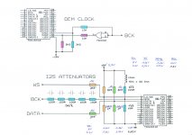
I attached latest DEM clock and I2S attenuator schematics. The I2S attenuators can also be used for the TDA1543.
The DEM clock circuit consists of two resistive attenuators that perform biasing, level-shifting and attenuation. The DEM clock frequency has been increased to 2.8224 MHz (bit clock).
The I2S attenuators provide both a bias voltage (approx. 1.2V), and attenuation of the I2S signals. By lowering I2S signal amplitude, sound get's much more refined, due to reduction of I2S interference.
The bit clock (BCK) attenuator needs a choke (10mH Panasonic ferrite-core choke) to attenuate power supply noise. This choke will also provide a high impedance to +5V, so the series resistor value can be increased, and the shunt resistor value can be lowered.
I used multiple 100R resistors in order to minimize the effect of resistor stray capacitance.
I tried many, more complicated discrete designs. This simple circuit performs best so far, especially when using multiple low noise transistors in parallel, minimizing current flow through each transistor.
The simple trans-impedance I/V converter uses current steering and is extremely fast (large bandwidth). By using few high quality (low noise) parts, signal degradation can be minimized.
Single-ended output (class A) seems to provide cleanest sound, as cross-over distortion is eliminated.
I implemented the above I2S atteunators and it works, but when i conect the DEM clock as shown there was a lot of noise. I even conected the +5V supply to Pin 14 and Gnd to Pin 7.
What is wrong?
Help greatly appreciated
Attachments
Last edited:
Hi John,
thank you for answers.
I'm totaly off topic here : I found your first SDplayer (than I didn't hear) very smaryt because also the librairy management with the SD card. I know you choose it because the jitter, but was not a bad idea either for the lover of music to have SD cards for travelling with portable devices as it's lighter than a 2.5 DD !
Why not push the concept with a RJ45 input and a free embeded linux solution for library management à la Squeezebox server with PDA as remotecontrol. Mini USB is cute but a little fragile , that's my own experience with PDAs....
Maybe as an option on your devices ! I love the boxes, you have a great sense of design not only for the Layout.
regards
Thank you for sharing.
Last edited:
Hi Ceglar:
If tests with Ian’s FIFO reclocker and simultaneous mode lead to max. 192 KHz sample rate (asuming clock generation and distribution is correct). Then 32 bits are clocked in simultaneously and truncated by the TDA1541A at a bit clock rate equal to the sample rate multiplied by 32. This would result in 6.144 MHz bit clock rate and that’s just within TDA1541A clock specs.
Standard TDA1541A application with 4 times oversampling, I2S interface and 32 bits / frame (SAA7220) results in 176.4 KHz sample rate and 5.6448 MHz bit clock rate. 192 KHz would result in 6.144 MHz bit clock and that’s the same bit clock frequency as with Ian’s FIFO module outputting 32 bits in simultaneous mode.
Simultaneous mode was included for 8 times oversampling with only 16 bits clocked in for L channel and 16 bits clocked in for R channel simultaneously with 5.6448 MHz bit clock rate. This would result in 352.8 KHz sample rate (44.1 KHz, 8 times ooversampling).
The theoretical maximum sample rate that still falls within TDA1541A clock specs equals 6.4 MHz / 16 = 400 KHz, 384 KHz sample rate falls within TDA1541A clock specs.
Not yet, in order to do so one will need a suitable I2S source that only clocks out 16 bits (offset binary) without truncating with matching bit clock and I don’t have such source.
I already tested lower bit clock rates with the first SD-player that outputs 32 bits / frame with 1.4112 MHz bit clock.
phase noise of a clock divided by two will theoretically be 6dB lower than the phase noise of the original clock signal.
http://www.silabs.com/Support Documents/TechnicalDocs/Clock-Division-WP.pdf
Look at page 4.
So with bit clock frequency halved, we could measure lower jitter, depending on divider cycle to cycle jitter. Perhaps lower than with most of the I2S sources that output 64 bits/frame.
Pedja reported lower deterministic jitter, this could also be a result of relatively long I2S interlinks (FIFO reclocker connected to a separate DAC module) that do not run over a solid ground plane. Now a lower bit clock rate would lead to less crosstalk (asuming stray capacitance remains the same) and thus also lower deterministic jitter.
In simultaneous mode (pin 27 connected to -5V) the input register is split up from a single 64 bits register into two separated 32 bit registers. These are the same registers that are also used for I2S. Data is now clocked in through pins 3 & 4 into first and second 32 bits input register simultaneously. After LE goes low, the first rising edge of BCK will latch the values of both input register in the same output register. So everything is the same as with I2S, except for the splitting up of the input register. So I see no reason why this would have big impact on deterministic jitter (apart from the lower bit clock of course) as the same registers and latches are used, and the output still latches on the rising edge of BCK.
Surely thats 192kHz.
If tests with Ian’s FIFO reclocker and simultaneous mode lead to max. 192 KHz sample rate (asuming clock generation and distribution is correct). Then 32 bits are clocked in simultaneously and truncated by the TDA1541A at a bit clock rate equal to the sample rate multiplied by 32. This would result in 6.144 MHz bit clock rate and that’s just within TDA1541A clock specs.
Standard TDA1541A application with 4 times oversampling, I2S interface and 32 bits / frame (SAA7220) results in 176.4 KHz sample rate and 5.6448 MHz bit clock rate. 192 KHz would result in 6.144 MHz bit clock and that’s the same bit clock frequency as with Ian’s FIFO module outputting 32 bits in simultaneous mode.
Simultaneous mode was included for 8 times oversampling with only 16 bits clocked in for L channel and 16 bits clocked in for R channel simultaneously with 5.6448 MHz bit clock rate. This would result in 352.8 KHz sample rate (44.1 KHz, 8 times ooversampling).
The theoretical maximum sample rate that still falls within TDA1541A clock specs equals 6.4 MHz / 16 = 400 KHz, 384 KHz sample rate falls within TDA1541A clock specs.
Have you measured jitter levels between the two modes of operation?
Not yet, in order to do so one will need a suitable I2S source that only clocks out 16 bits (offset binary) without truncating with matching bit clock and I don’t have such source.
I already tested lower bit clock rates with the first SD-player that outputs 32 bits / frame with 1.4112 MHz bit clock.
phase noise of a clock divided by two will theoretically be 6dB lower than the phase noise of the original clock signal.
http://www.silabs.com/Support Documents/TechnicalDocs/Clock-Division-WP.pdf
Look at page 4.
So with bit clock frequency halved, we could measure lower jitter, depending on divider cycle to cycle jitter. Perhaps lower than with most of the I2S sources that output 64 bits/frame.
Pedja reported lower deterministic jitter, this could also be a result of relatively long I2S interlinks (FIFO reclocker connected to a separate DAC module) that do not run over a solid ground plane. Now a lower bit clock rate would lead to less crosstalk (asuming stray capacitance remains the same) and thus also lower deterministic jitter.
In simultaneous mode (pin 27 connected to -5V) the input register is split up from a single 64 bits register into two separated 32 bit registers. These are the same registers that are also used for I2S. Data is now clocked in through pins 3 & 4 into first and second 32 bits input register simultaneously. After LE goes low, the first rising edge of BCK will latch the values of both input register in the same output register. So everything is the same as with I2S, except for the splitting up of the input register. So I see no reason why this would have big impact on deterministic jitter (apart from the lower bit clock of course) as the same registers and latches are used, and the output still latches on the rising edge of BCK.
Hi Audiohifi,
Circuit lay-out is -very- critical, one would have to place the complete circuit (especially the DEM clock circuit) over a solid ground plane and use shortest possible wiring (millimeters) and effective decoupling. Failing to do so causes instabilities (noise).
I now use a free running low jitter DEM oscillator:
470pF film cap between pin 16 & 17.
6K8 resistor between pin 15 & 16.
6K8 resistor between pin 15 & 17.
The latest I2S attenuators I used were diode attenuators:
Diode #1, cathode to I2S source, anode to TDA1541A I2S input.
Diode #2 … #4 in series, cathode to ground, anode to TDA1541A I2S input.
Pull up resistor, 1K for WS and DATA, 330R for BCK between +5V and TDA1541A I2S input.
1N4148 diodes will do fine. One could also use an IR led (1V2) with a diode in series to replace the 3 diode diodes in series. Impedance would be a bit lower this way.
These diode attenuators produce a very clean 1V2pp I2S signal that varies between 0V6 and 1V8.
The pull-up resistors may pollute the 5V power supply. One could use split pull-up resistors (470R, 470R for example) and decouple the junction to GND using a capacitor.
I implemented the above I2S attenuators and it works, but when i conect the DEM clock as shown there was a lot of noise. I even conected the +5V supply to Pin 14 and Gnd to Pin 7.
What is wrong?
Help greatly appreciated
Circuit lay-out is -very- critical, one would have to place the complete circuit (especially the DEM clock circuit) over a solid ground plane and use shortest possible wiring (millimeters) and effective decoupling. Failing to do so causes instabilities (noise).
I now use a free running low jitter DEM oscillator:
470pF film cap between pin 16 & 17.
6K8 resistor between pin 15 & 16.
6K8 resistor between pin 15 & 17.
The latest I2S attenuators I used were diode attenuators:
Diode #1, cathode to I2S source, anode to TDA1541A I2S input.
Diode #2 … #4 in series, cathode to ground, anode to TDA1541A I2S input.
Pull up resistor, 1K for WS and DATA, 330R for BCK between +5V and TDA1541A I2S input.
1N4148 diodes will do fine. One could also use an IR led (1V2) with a diode in series to replace the 3 diode diodes in series. Impedance would be a bit lower this way.
These diode attenuators produce a very clean 1V2pp I2S signal that varies between 0V6 and 1V8.
The pull-up resistors may pollute the 5V power supply. One could use split pull-up resistors (470R, 470R for example) and decouple the junction to GND using a capacitor.
Hi Eldam,
The SD-transport has a number of advantages:
- Saves a lot of energy (SD-transport consumes approx. 400 milliwatts during streaming). Computer or music server will consume much more power.
- Always provides bit-perfect playback.
- Guarantees that there are no “hidden” sample rate conversions like 44.1KHz > 48 KHz audio bus > 44.1KHz out for example.
- Fast response, switch on power, press play, music within seconds.
- Stand alone operation for purists that do not want to connect their audio equipment to computers / servers.
- Low jitter and a controllable and defined jitter spectrum.
- Single clock, all circuits work in the same time domain, no crosstalk and related issues.
- Compact, portable, durable.
- Like Vinyl, tape and CD you have your music on a piece of hardware (SD-card).
UD1 and UD2 circuits (asynchronous, slaved USB receiver chip inclusive) all run on a single 48 MHz masterclock. Similar to the SD-transport, all circuits will operate in the same time domain and there is no crosstalk between multiple clocks.
When using wired network, multiple clocks and crosstalk between these clocks are unavoidable. This always causes degrading compared to a single clock concept. Even if WIFI is used, multiple clocks are unavoidable and the impact of WIFI (EMI) on the entire audio set (including speaker external and internal unscreened wiring) is unavoidable too.
The standard for most devices is micro USB, these connectors are even smaller than mini USB and are often used to charge devices like smartphones and pads. When the mini USB socket gets broken it can be replaced. Unlike with mass produced stuff like smartphones and pads I use overdimensioded solder pads and manual soldering to ensure these mini USB sockets are mounted firmly to the PCB. When a poor contact may occur, the mini USB socket can be easily replaced.
I'm totaly off topic here : I found your first SDplayer (than I didn't hear) very smaryt because also the librairy management with the SD card. I know you choose it because the jitter, but was not a bad idea either for the lover of music to have SD cards for travelling with portable devices as it's lighter than a 2.5 DD !
The SD-transport has a number of advantages:
- Saves a lot of energy (SD-transport consumes approx. 400 milliwatts during streaming). Computer or music server will consume much more power.
- Always provides bit-perfect playback.
- Guarantees that there are no “hidden” sample rate conversions like 44.1KHz > 48 KHz audio bus > 44.1KHz out for example.
- Fast response, switch on power, press play, music within seconds.
- Stand alone operation for purists that do not want to connect their audio equipment to computers / servers.
- Low jitter and a controllable and defined jitter spectrum.
- Single clock, all circuits work in the same time domain, no crosstalk and related issues.
- Compact, portable, durable.
- Like Vinyl, tape and CD you have your music on a piece of hardware (SD-card).
Why not push the concept with a RJ45 input and a free embeded linux solution for library management à la Squeezebox server with PDA as remotecontrol. Mini USB is cute but a little fragile , that's my own experience with PDAs….
UD1 and UD2 circuits (asynchronous, slaved USB receiver chip inclusive) all run on a single 48 MHz masterclock. Similar to the SD-transport, all circuits will operate in the same time domain and there is no crosstalk between multiple clocks.
When using wired network, multiple clocks and crosstalk between these clocks are unavoidable. This always causes degrading compared to a single clock concept. Even if WIFI is used, multiple clocks are unavoidable and the impact of WIFI (EMI) on the entire audio set (including speaker external and internal unscreened wiring) is unavoidable too.
The standard for most devices is micro USB, these connectors are even smaller than mini USB and are often used to charge devices like smartphones and pads. When the mini USB socket gets broken it can be replaced. Unlike with mass produced stuff like smartphones and pads I use overdimensioded solder pads and manual soldering to ensure these mini USB sockets are mounted firmly to the PCB. When a poor contact may occur, the mini USB socket can be easily replaced.
Hi John,
Appreciate the reply, you give a lot.
It would be for a single PCB where the layout could be assumed to be quite good. I understand this was for his Model S DAC with USB input. My interest with the Simultaneous mode lies in PC software up sampling to 192kHz. It would interesting to hear back about what you find re: measurements if you go down this path.
If I can.. What would you consider to be an appropriate corner frequency for analog low pass filter with NON-OS 1541A?. Seems it varies from 100kHz to 400kHz and possibly higher, and not only am I clueless wrt this, but there doesn't appear to be much info out there either, it might serve to help our Archives if you can spare a minute or two.
Lastly, its so encouraging to see a resurgence of interest in 1541A, and ambition with ways in which it can be utilised.
Thank you,
Shane
Appreciate the reply, you give a lot.
Hi Ceglar:
Pedja reported lower deterministic jitter, this could also be a result of relatively long I2S interlinks (FIFO reclocker connected to a separate DAC module) that do not run over a solid ground plane. Now a lower bit clock rate would lead to less crosstalk (asuming stray capacitance remains the same) and thus also lower deterministic jitter.
It would be for a single PCB where the layout could be assumed to be quite good. I understand this was for his Model S DAC with USB input. My interest with the Simultaneous mode lies in PC software up sampling to 192kHz. It would interesting to hear back about what you find re: measurements if you go down this path.
If I can.. What would you consider to be an appropriate corner frequency for analog low pass filter with NON-OS 1541A?. Seems it varies from 100kHz to 400kHz and possibly higher, and not only am I clueless wrt this, but there doesn't appear to be much info out there either, it might serve to help our Archives if you can spare a minute or two.
Lastly, its so encouraging to see a resurgence of interest in 1541A, and ambition with ways in which it can be utilised.
Thank you,
Shane
Last edited:
I used I2S splitter from L/R to L/L and R/R long tine ago.
with same shift register chips but HEF version. Was working even with higher sample rates
than 44.1. But I spot that the speed depends on power supply value. So from datasheets it could be higher as 12V. I run HEF on 8 to 9V...
Circuit was driving 2 x sabre ess9008 factory setting chip dual mono, all parallel, mode.
It was more than good
The pull-up resistors may pollute the 5V power supply. One could use split pull-up resistors (470R, 470R for example) and decouple the junction to GND using a capacitor.
How about a seperate +5V regulator for the pull up resistors?
Koldby
Hi Ceglar,
The remark from Pedja about reducing crosstalk made me wonder what happens when BCK is shut down during the time the redundant bits 16 … 31 would be clocked in.
This would theoretically halve crosstalk and switching noise as BCK would be shut down half of the time. This means that during half of the sample time, switching noise would be eliminated.
I just performed an experiment with bit clock stopping. Here the bit clock is only enabled during the time bits 0 … 15 are clocked in, it is shut down during the time the remaining bits 16 … 31 would be clocked in as the TDA1541A is only 16 bits.
I connected a synchronous divider (divide by 32 using Q4 output) to BCK and reset it using a short pulse from a one shot generator connected to WS in order to synchronise the divider with WS. The divider Q4 output creates a signal that is only high when bits 0 … 15 need to be clocked in.
The divider output was then connected to a BCK diode attenuator. The BCK signal is present when the pull up resistor is pulled high by the divider output.
The clock stopper could be switched on and off by connecting the pull up resistor either to +5V (continuous BCK clock) or to the divider output (clock stopping). This way the impact of the BCK circuit during comparison is minimised.
Measurements with the scope revealed switching noise on the TDA1541A output during the time bits 0 … 15 are clocked in and silence when BCK is stopped. With continuous BCK clock signal, switching noise was present during the entire sample period.
Hi koldby,
This works but there could still be crosstalk between BCK and DATA signals (deterministic jitter) through this extra 5V regulator (same when using TDA1541A 5V supply). By using the split pull up resistor with a decoupling cap on the junction of both resistors this crosstalk can be significantly reduced while the 5V supply stays clean too.
How about a seperate +5V regulator for the pull up resistors?
This works but there could still be crosstalk between BCK and DATA signals (deterministic jitter) through this extra 5V regulator (same when using TDA1541A 5V supply). By using the split pull up resistor with a decoupling cap on the junction of both resistors this crosstalk can be significantly reduced while the 5V supply stays clean too.
Your Latest I2S Atteunator
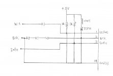
Hi John,
Thank you for your reply.
See attachment. Is my understanding correct.
Hi Audiohifi,
Circuit lay-out is -very- critical, one would have to place the complete circuit (especially the DEM clock circuit) over a solid ground plane and use shortest possible wiring (millimeters) and effective decoupling. Failing to do so causes instabilities (noise).
I now use a free running low jitter DEM oscillator:
470pF film cap between pin 16 & 17.
6K8 resistor between pin 15 & 16.
6K8 resistor between pin 15 & 17.
The latest I2S attenuators I used were diode attenuators:
Diode #1, cathode to I2S source, anode to TDA1541A I2S input.
Diode #2 … #4 in series, cathode to ground, anode to TDA1541A I2S input.
Pull up resistor, 1K for WS and DATA, 330R for BCK between +5V and TDA1541A I2S input.
1N4148 diodes will do fine. One could also use an IR led (1V2) with a diode in series to replace the 3 diode diodes in series. Impedance would be a bit lower this way.
These diode attenuators produce a very clean 1V2pp I2S signal that varies between 0V6 and 1V8.
The pull-up resistors may pollute the 5V power supply. One could use split pull-up resistors (470R, 470R for example) and decouple the junction to GND using a capacitor.
Hi John,
Thank you for your reply.
See attachment. Is my understanding correct.
Attachments
- Home
- Source & Line
- Digital Line Level
- Building the ultimate NOS DAC using TDA1541A