Hi qusp,
The zener noise is filtered by a RC filter (330R / 470uF), then buffered by a Darlington.
I used these circuits based on perceived sound quality. They offer very low noise and fast local current feedback.
The trimmers are Bourns cermet multiturns. Their output voltage is also filtered. For the MOSFET current buffer I use 250K trimmer with 1uF SMD film cap and for the DC reference voltage I use 1K trimmer with 470uF Sanyo Oscon capacitor
John, can buried zeners or other forms of reference be used for lower noise? i guess there is some reason you chose straight zeners though, no feedback perhaps?
The zener noise is filtered by a RC filter (330R / 470uF), then buffered by a Darlington.
I used these circuits based on perceived sound quality. They offer very low noise and fast local current feedback.
nice one, ive been using those panasonic pps for a while now too, very nice caps. cool looking module for sure; i pictured you using bulk foil trimmers =)
The trimmers are Bourns cermet multiturns. Their output voltage is also filtered. For the MOSFET current buffer I use 250K trimmer with 1uF SMD film cap and for the DC reference voltage I use 1K trimmer with 470uF Sanyo Oscon capacitor
Hi JOSI1
They offer a very high level of reliability and are only used in less critical positions.
Plain SMD resistors need to be positioned with the text facing upwards for easy inspection. This takes extra time during manual assembly.
In your designs you are using MELF resistors. Do these resistors have an electrical advantage compared to 0805/1210 or is it just for easier/better mounting and soldering?
They offer a very high level of reliability and are only used in less critical positions.
Plain SMD resistors need to be positioned with the text facing upwards for easy inspection. This takes extra time during manual assembly.
Hi John,
in post #4000 so mention that you are using a separate transformer (2x12V) for the power supply of the SD-Transport (3V3). Do You use the same common mode voltage regulator concept as for the MK8?
Which part of the power supply is already located on the latest SD-Transport module and which part has to be realized externally (transformer, rectifier, smoothing cap, common mode cap multiplier, ???)
Hi John, can you explain us a bit about your grounding philosophy?
I see the supply lines being decoupled to gnd just after the regulators. You also mentioned your grounding for the tda (using separate lines running to pin 5). How are you using the top plane?
-----
Further to this, I had a closer look at the layout... It seems like:
- ...+5V (Reclocker) and -15V are decoupled to the same GND line
- ...-5V supply is decoupled to the GND belonging to the -15V supply?
- ...all GND lines in the supplies are connected to a common GND plane (top)
- ...decoupling of the supply lines to the chip is done quite far away from the TDA
:Confused:
Hi studiostevus,
All common mode voltage regs on the MK8 are decoupled with 1uF SMD film cap close to the regulator output. There are no electrolytic caps on the regulator outputs.
The references of all 4 common mode voltage regulators are connected to the ground plane that serves as GND reference:
Masterclock, synchronous BCK divider and synchronous WS / DATA reclockers all have local RC filters located very close to these circuits. The resistor for the masterclock RC power supply filter is a low noise Honeycomb Mobius resistor.
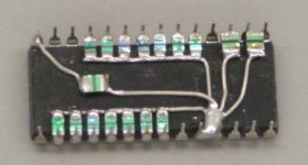
The TDA1541A power supply SMD film decoupling caps are soldered directly to the chip pins, underneath the chip as close to the IC housing as possible (attached picture).
So TDA1541A power supply decoupling is actually pretty close to the chip.
The 14 active divider decoupling caps are also soldered directly to the TDA1541A pins. Only 14 pins of the TDA1541A are connected to the MK8 module using a customized IC socket.
Further to this, I had a closer look at the layout... It seems like:
...+5V (Reclocker) and -15V are decoupled to the same GND line
...-5V supply is decoupled to the GND belonging to the -15V supply?
...all GND lines in the supplies are connected to a common GND plane (top)
...decoupling of the supply lines to the chip is done quite far away from the TDA
All common mode voltage regs on the MK8 are decoupled with 1uF SMD film cap close to the regulator output. There are no electrolytic caps on the regulator outputs.
The references of all 4 common mode voltage regulators are connected to the ground plane that serves as GND reference:
Masterclock, synchronous BCK divider and synchronous WS / DATA reclockers all have local RC filters located very close to these circuits. The resistor for the masterclock RC power supply filter is a low noise Honeycomb Mobius resistor.
The TDA1541A power supply SMD film decoupling caps are soldered directly to the chip pins, underneath the chip as close to the IC housing as possible (attached picture).
So TDA1541A power supply decoupling is actually pretty close to the chip.
The 14 active divider decoupling caps are also soldered directly to the TDA1541A pins. Only 14 pins of the TDA1541A are connected to the MK8 module using a customized IC socket.
Attachments
Hi JOSI1
Yes, the SD-transport runs on a similar common mode power supply consisting of a common mode capacitance multiplier driving a common mode 3.3V filtered buffered zener regulator.
The binary stepped shunt volume control still runs on conventional 3.3V and 5V power supplies that will also be replaced with common mode power supplies.
There will be 3 small toroidal transformers in total. One 2 x 12V transformer is used for isolated +5V and -5V supply for the DAC chip. One 2 x 18V transformer is used for isolated -15V supply for the DAC chip and isolated +5V supply for masterclock and connected circuits. The third 2 x 12V transformer is used for isolated 3.3V supply for the SD-transport.
The SD-transport MK2 module will need a small add-on module that contains a 3.3V common mode voltage regulator. I am currently using an air wired setup for testing.
Transformers, rectifiers and common mode capacitance multipliers will all be located on the power supply module. These are the parts that need to be added externally.
in post #4000 so mention that you are using a separate transformer (2x12V) for the power supply of the SD-Transport (3V3). Do You use the same common mode voltage regulator concept as for the MK8?
Yes, the SD-transport runs on a similar common mode power supply consisting of a common mode capacitance multiplier driving a common mode 3.3V filtered buffered zener regulator.
The binary stepped shunt volume control still runs on conventional 3.3V and 5V power supplies that will also be replaced with common mode power supplies.
There will be 3 small toroidal transformers in total. One 2 x 12V transformer is used for isolated +5V and -5V supply for the DAC chip. One 2 x 18V transformer is used for isolated -15V supply for the DAC chip and isolated +5V supply for masterclock and connected circuits. The third 2 x 12V transformer is used for isolated 3.3V supply for the SD-transport.
Which part of the power supply is already located on the latest SD-Transport module and which part has to be realized externally (transformer, rectifier, smoothing cap, common mode cap multiplier, ???)
The SD-transport MK2 module will need a small add-on module that contains a 3.3V common mode voltage regulator. I am currently using an air wired setup for testing.
Transformers, rectifiers and common mode capacitance multipliers will all be located on the power supply module. These are the parts that need to be added externally.
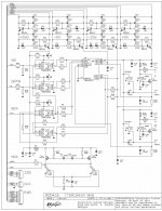
MK8 concept schematics.
I attached TDA1541A-MK8 concept schematics.
On the top there are 4 common mode voltage regulators for +5V, -5V, -15V, and +5V. They consist of cascaded filtered buffered zener diode regulators.
This works as follows, T1 and D5 form a 10V - 1.2V = 8.8V pre regulator. This pre regulator is placed in the ground reference line. T5 and D1 form a 6.2V - 1.2V = 5V post regulator that is referenced to the 8.8V GND reference provided by the pre regulator. R7 and C23 filter the zener diode noise.
The 5V post regulator is placed after the 8.8V pre regulator and re-stabilizes it to +5V. The output of the 8.8V pre regulator serves as ground reference. The output of the post regulator is decoupled to GND by a 1uF SMD film cap (C11).
The negative common mode voltage regulators function similar. The -15V regulator has a -18.8V pre regulator and a -15V post regulator.
Note that all common mode regulators have separate plus and minus inputs that are connected to the main power supply using twisted pairs. The main power supply contains rectifiers, smoothing caps and common mode capacitance multipliers.
WS and DATA inputs are first attenuated by R23 ... R26. U2 and U3 perform synchronous reclocking. R19, R20, R40 and R41 perform I2S attenuation for the TDA1541A. The MK8 only has 2 I2S inputs, DATA and WS. Source BCK signal is not connected to the module.
Each synchronous reclocker has a separate RC power supply filter, R21, C8, R22, C9.
BCK is derived from the masterclock using a synchronous Johnson counter consisting of U4 and U5. R28 ... R30 reduce ground bounce. R5 and R16 form the BCK I2S attenuator.
Balanced DEM clock is now derived from U5 using R43, R44, R31 and R32 to inject the signal into the DEM oscillator circuit on the TDA1541A.
The masterclock is built around 2 lateral MOSFETs T11 and T12. Both crystals are matched high-Q versions.
Chokes N1 and N2 are now connected to a DC reference voltage generated by R6 and C21. This lifts the clock signal above GND so clock rectifiers are no longer required. The masterclock runs on approx. 2V. CLC filter consisting of C12, R3 and C20 offers extra filtering of the 5V masterclock supply.
I/V conversion is passive by generating a voltage across resistors R17 and R18. The TDA1541A output current is buffered by lateral MOSFETs T9 and T10 that serve as current buffers (grounded gate circuit). The DC bias level on the TDA1541A outputs is adjusted by integrating the output signal across the passive I/V resistor and feeding it back to the MOSFET gate. This is done by P3, P4, C16 and C18. R45 and R46 make sure the MOSFETs can't go out of conduction as the DAC output current approaches zero.
The bias current running through the I/V resistors equals 2mA, so the DC voltage at the outputs equals +4V. In order to provide DC-coupled outputs, two +4V reference voltages are added that now serve as output "GND". The DC voltage between this DC reference and the voltage on the I/V resistor now equals 0V.
R1 and R2 are mobius loops that are used for low level refinement.
The MK8 outputs can be directly coupled to RCA sockets without the need of an additional module like required with the MK7.
Attachments
Hi John,
I find it interesting to follow the progression of circuit refinement from the earliest version of your DAC to the Mk8. While many engineers would probably find ways to add circuitry in an effort to "improve" performance, you continually find thoughtful and creative ways to distill the design down to it's essence. As Einstein reportedly said; everything should be as simple as possible, but not more simple.
I'm curious to know, which currently in production DAC chip would you choose to base a new DAC board design around if you could no longer obtain legitimate TDA1541x devices?
Last edited:
which currently in production DAC chip would you choose to base a new DAC board design around if you could no longer obtain legitimate TDA1541x devices?
Another Dutch company, Metrum Acoustics, introduced a 24/96 pure NOS DAC named 'NOS Mini DAC': No idea what chips are being used inside? AD55xx? anyone?
Another Dutch company, Metrum Acoustics, introduced a 24/96 pure NOS DAC named 'NOS Mini DAC': No idea what chips are being used inside? AD55xx? anyone?
I think it are DAC8580 from TI.

I think it are DAC8580 from TI.
I just had a quick look at the DAC8580 datasheet. The specification that jumps out as being relatively poor was the THD. T.I. lists a figure of -72dB for each of the first three harmonics(presumably, at full scale, and not linearized in software), which is 20dB (10x) or more worse than for the TDA1541A or the PCM56. Also, no THD figures appear to be presented for test signals at -20dB and -60dB levels.
Last edited:
Hi John,
I'm curious to know, which currently in production DAC chip would you choose to base a new DAC board design around if you could no longer obtain legitimate TDA1541x devices?
Given that there were million of the tda1541x produced, it isn't difficult to find a legitimate one, unless you need quantities for something other than diy?
Given that there were million of the tda1541x produced, it isn't difficult to find a legitimate one, unless you need quantities for something other than diy?
WERE a million, does seem to be the operative point. I suppose that my real question was what would John select among the current production DACs if forced to, and not so much a statement about the availability of the TDA1541A. However, when ventures a small as Pedja Rogic's Audial announce that they will be moving away from the TDA1541A due to questionable sourcing and availability, I'd say that suggests there is issue is of real concern for both commercial and DIY consumers.
The specification that jumps out as being relatively poor was the THD. T.I. lists a figure of -72dB for each of the first three harmonics(presumably, at full scale, and not linearized in software)
I didn't consider the full-scale THD to be a big show stopper. What disinclined me from getting some of these chips to play with was the glitch energy. Looking closer it seems the software linearization (which must be performed externally, weird they mention it in the datasheet) makes low level performance worse.
Hi Ken Newton,
Probably the PCM1704. The Arda Technologies AT1401 looks promising but I am not sure IF or when it becomes available.
I'm curious to know, which currently in production DAC chip would you choose to base a new DAC board design around if you could no longer obtain legitimate TDA1541x devices?
Probably the PCM1704. The Arda Technologies AT1401 looks promising but I am not sure IF or when it becomes available.
WERE a million, does seem to be the operative point. I suppose that my real question was what would John select among the current production DACs if forced to, and not so much a statement about the availability of the TDA1541A. However, when ventures a small as Pedja Rogic's Audial announce that they will be moving away from the TDA1541A due to questionable sourcing and availability, I'd say that suggests there is issue is of real concern for both commercial and DIY consumers.
Well the alternatives would all have the I2S left/right issue, in other words you have to muck up the I2s to get the L&R Dac's in synch.
But one of the other TDA1541 experts posted this a few years ago (I forget whom.):
DAC THD&N SNR
AD1865 - 88dB -110dB
AD1862 - 98dB -119dB
PCM56 - 94dB -110dB
PCM63 - 92dB -120dB
PCM1704 - 92dB -120dB
TDA1541A -100dB -110dB
TDA1543 - 75dB - 96dB
TDA1545A - 88dB -101dB
Seeing this table shows the TDA1541A as actually having the lowest THD & N at full scale. The AD1862 and PCM56 are second and third respectively, followed by the newer BB PCM Chips and with the AD1865 and TDA1545 bringing up the rear with the almost poorest performance, but that honour actually goes to the TDA1543.
So, my first suggestion, if one is desirous of a high quality NON-OS DAC is to select one that uses DAC's that have a low THD & N, which seems to limit us to TDA1541A, PCM56 and AD1862. It would also seem that it is best to avoid the TDA1543, and probably too the TDA1545A and the AD1865.
When you start looking at -10 dB THD+N the 1541 gap gets bigger. Plus profile of those THD numbers at different harmonics, there just isn't a sub.
Now many take the AD1862 as very well designed (Jocko I believe is a big fan). Also Erno Borbely told me he believes the PCM1704 is the best. The PCM56 has been least evil sub as its only recently went out of production. But the problem with any of these choices and NOS is the L&R issue. Hopefully one day we will manage to have a computer transport that can spit out Phillips I2s 24 bit slaved by the DAC clock with the option to split the L&R channels. This hasn't even been close to have been accomplished. There is one pretty innovative commercial USB NOS PCM1704 Dac that people are raving about, but nothing worth a damn IMHO has been made public for DIY.
So I guess what I am saying is go to a few garage sales till you find an old CDP with a TDA1541A and keep the thread on topic, I don't see what is so hard about it unless you have a commercial motive.
My assault on the K8 version recloker
An externally hosted image should be here but it was not working when we last tested it.
An externally hosted image should be here but it was not working when we last tested it.
An externally hosted image should be here but it was not working when we last tested it.
Last edited:
Regal,
The practical reality is that the 11uS temporal channel displacement of the multiplexed 44.1kHz rate L/R is inconsequential. The spatial displacement is 15/100ths of an inch. I very much doubt that your speakers are equidistant from your listening position to less than that, and even if you carefully made them so you would have to lock your head in a vise to maintain such an equidistance.
I'm rather certain that the quote you included is by Thorsten Loesch. I'm not sure how you could have cut-and-pasted it without obviously seeing who the author is.
According to T.I.'s website, the PCM56 continues to be in production. Not sure where you heard otherwise.
Lastly, I must tell you that I find your attempts to play thread police by admonishing me to, in your view, "keep the thread on topic", and your continued suggestion that because YOU can't imagine any reason other than a commercial one for my question must therefore mean it is also MY reason, are rediculous and mildly offensive. In the future, if you don't know what you are talking about, which you clearly don't here, then please don't respond to questions which are not directed to you.
Last edited:
- Home
- Source & Line
- Digital Line Level
- Building the ultimate NOS DAC using TDA1541A