Hi -EC-,
Thanks for your reply on post #3459.
You see, I predicted your move")
The low value stop gate resistor allows for paralleling resistance wire in the Mobious loop. I bet that will improve the sound! ...being in the signal path...
The synchronous recloker circuit looks rather easy to build, from here...I have to use it on my (now neglected) CD-PRO.
I have little time to DIY nowadays; I will be devoted to build decent boxes to -ECdesigns- DACs, now that all have honeycomb resistors.
Best of lucks.
M.
Thanks for your reply on post #3459.
I use 120R gate resistors in the prototype setup because of the long wires running to the powerFET gates. I plan to use wirewound resistors (Tyco / Rhopoint) for the higher values up to 100K and Honeycomb / Mobius for the lower values up to 1K.
You see, I predicted your move
The low value stop gate resistor allows for paralleling resistance wire in the Mobious loop. I bet that will improve the sound! ...being in the signal path...
The synchronous recloker circuit looks rather easy to build, from here...I have to use it on my (now neglected) CD-PRO.
I have little time to DIY nowadays; I will be devoted to build decent boxes to -ECdesigns- DACs, now that all have honeycomb resistors.
Best of lucks.
M.
Question for you guys
Hi all,
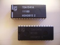
I have some units of the TDA1541A, and they all work. The dude is, if it is "remarked", because, it seems to be impossible that this chip was made from 2008, please, see enclosed. If someone knows something about this, just answer me please. I have 5 units manufactured from 2004, and they all work fine too. But these last ones I know that were made deliberately.
Kind regards,
Long life to the TDA1541
Hi all,
I have some units of the TDA1541A, and they all work. The dude is, if it is "remarked", because, it seems to be impossible that this chip was made from 2008, please, see enclosed. If someone knows something about this, just answer me please. I have 5 units manufactured from 2004, and they all work fine too. But these last ones I know that were made deliberately.
Kind regards,
Long life to the TDA1541
Attachments
Honeycomb / Mobius resistor wattage
Hi ppap64.
I use these resistors for passive I/V conversion, dissipation here is approx. 4 milliwatts. Wire is not used for providing high wattage but for achieving low noise levels.
Given a 500R Mobius / Honeycomb resistor made of 100 ohm/m Isotan resistance wire, power rating equals approx. 2.6 watts. This is based on wire temperature of approx. 100 degrees centigrade and 72mA running through the wire.
So a 100R Mobius resistor of the same wire could handle P = I * I * R = 0.072 * 0.072 * 100 = 518 mW.
Wattage can be increased by increasing wire diameter.
Here are indication currents (approx. 100 degrees centigrade wire temp) for different Isotan wire diameters:
0.5mm, (2.5 Ohms / meter), 608 mA
0.25mm, (10 Ohms / meter), 368 mA
0.15mm (28 Ohms / meter), 128 mA
0.1mm, (63 Ohms / meter), 76 mA
0.08mm, (100 Ohms / meter), 72 mA
500 Ohm Honeycomb resistor made from 200 meters of 0.5mm diameter Isotan would have power rating of approx. 184 watts.
Hi ppap64.
If you use 100 ohm/m Isotan to wind them, approx. what wattage
rating would they have?
I use these resistors for passive I/V conversion, dissipation here is approx. 4 milliwatts. Wire is not used for providing high wattage but for achieving low noise levels.
Given a 500R Mobius / Honeycomb resistor made of 100 ohm/m Isotan resistance wire, power rating equals approx. 2.6 watts. This is based on wire temperature of approx. 100 degrees centigrade and 72mA running through the wire.
So a 100R Mobius resistor of the same wire could handle P = I * I * R = 0.072 * 0.072 * 100 = 518 mW.
Wattage can be increased by increasing wire diameter.
Here are indication currents (approx. 100 degrees centigrade wire temp) for different Isotan wire diameters:
0.5mm, (2.5 Ohms / meter), 608 mA
0.25mm, (10 Ohms / meter), 368 mA
0.15mm (28 Ohms / meter), 128 mA
0.1mm, (63 Ohms / meter), 76 mA
0.08mm, (100 Ohms / meter), 72 mA
500 Ohm Honeycomb resistor made from 200 meters of 0.5mm diameter Isotan would have power rating of approx. 184 watts.
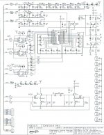
Final single TDA1541A DAC module, the TDA1541A-MK4.
After extensive (listening) tests and feedback from critical listeners, I decided the TDA1541A-MK4 will be the final single-TDA1541A DAC version.
I attached schematic diagram of the MK4.
Due to CAD system limitations, some parts appear double in the schematics (R15 ... R18 and R21 ... R24). This is caused by providing option for two different resistor types. In practice only 1 resistor is used.
Starting with the power supplies, +5V, -5V, and -15V regulators are same as with MK3 version, only ferrite beads are of different type.
The masterclock / bit reclocker supply filter has been modified to a 12th order LC low-pass. Additional voltage attenuators (D1, D11, D12 and D8, D9, D10, and D15) are used to derive required 2.4V / 2.5V for the synchronous reclockers.
TDA1541A decoupling caps are 47nF PPS 1206 size SMD, they are soldered underneath the TDA1541A for shortest possible wiring (RF decoupling).
DEM synchronizer consists of 2 Schottky diodes, 2 x 12K series resistors and 2 x 2K2 bias resistors. DEM clock rate = bit clock rate = 1.4112 MHz. because of this increased DEM clock rate, lower decoupling cap values can be used.
I/V conversion consists of 2 x 2SK170 in parallel (grounded-gate current buffer) driving a 500R passive I/V resistor. 5K wirewound bias resistors are added to ensure correct operation. Power amp (volume pot) connects between +5V and output. This removes +5V power supply from the direct signal path.
All I2S signals are now synchronously reclocked using very fast (low propagation delay / jitter) D flip-flops running on 2.4 ... 2.5V power supply.
latest I2S attenuators provide clean I2S signals that vary between +0.6V and +1.8V. This keeps on-chip ground-bounce low.
The new balanced masterclock with 2 outputs drives SD-transport and bit reclocker (only 1 clock load on each output). The crystals must be closely matched (same batch) and should have high Q factor.
Clock rectifiers D16 / R8 and D17 / R9 block the negative signal half of the masterclock outputs.
All chokes and masterclock / bit reclocker circuits are shielded.
The perceived sound quality from this MK4 is highly transparent and very natural. There are no audible (digital) artefacts nor "edge". Sound is very smooth, yet transient response is still fast. Due to the extreme black background (virtually inaudible background noise level), all details that are on a recording, including recording noise floor / spectrum will be clearly audible.
The MK4 forced me to tackle my power amps once again. The 8 FETs in the bridge power amps now limit dynamic resolution. First solution was a 6 FET Circlotron bridge power amp, yet even 6 FETs turned out to be too much (dynamic resolution appears to degrade with increased number of semiconductors in the signal path).
This lead to a 4 FET Circlotron power amp design with SE / Balanced inputs. It's based on 1 x 2SJ109 and 2 x 2SK1530. Rated output power is around 40 watts rms in 8 Ohms.
I am also experimenting with 10K wirewound volume pots. First impression is that they are more transparent and detailed compared to ALPS blue. The wirewound pot inductance (actually rather low, in the uH range), doesn't seem to affect the audio spectrum.
Attachments
> This lead to a 4 FET Circlotron power amp design with SE / Balanced inputs. It's based on 1 x 2SJ109 and 2 x 2SK1530. Rated output power is around 40 watts rms in 8 Ohms.
Something like this ?
http://www.diyaudio.com/forums/pass-labs/78734-new-tron-2.html#post925332
Something like this ?
http://www.diyaudio.com/forums/pass-labs/78734-new-tron-2.html#post925332
Hi EUVL,
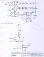
No it's quite different, I attached a concept schematic I am experimenting with.
Power supplies first, there are 2 main power supplies for the Circlotron (built around transformers N1 and N2). I used separate transformers instead of dual secondary windings in order to eliminate side effects of 5 ... 10nF typical stray capacitance between windings. This stray capacitance appears between both speaker terminals. Classical Circlotron stage requires 2 fully isolated power supplies.
The third power supply is for the input / driver stage only. First I remove ripple voltage (T1 and T2), next I create +20V, +15V, and -15V stabilized power supplies. The +15V (5V potential difference with +20V) is used as input reference voltage in order to enable sufficient output swing with this circuit.
By using a dedicated power supply for the driver stage, supply quality is not affected by the power stage. This enables very clean signal, even at high power levels. It also reduces both hum and noise to inaudible levels.
The circlotron power amp is about as basic as it gets. Plain differential stage (T3), DC-offset pot, bias pot and some chokes for both filtering and thermal compensation (PTC). Required gain is rather low (10 ... 20x) so a single differential pair will do fine.
Note that my main objective is obtaining highest possible resolution / best possible tracking of complex dynamic signals, not ultra low THD at 1 KHz sine wave.
The DC offset pot P2 is required to trim DC offset voltage across the speaker to lowest possible value. P1 sets exact bias current through the input / driver stage, and as a result of this, also the DC voltage drop across R8 and R9. These in turn control the bias current in the Circlotron power stage by varying Ugs.
I have around 17mA bias current running through R3. I use a watt meter to get some feedback about the bias current running through the Circlotron stage (approx. 150mA for each powerFET).
There is one catch with this simple input / driver circuit, symmetry. When driving this stage with a SE input signal, the ac voltage across R8 will be higher than the ac voltage across R9. Simply changing resistance value for either resistors would lead to imbalance in power stage bias currents as these are derived from voltage drop across these resistors.
So I used a RC circuit in parallel with R8 in order to maintain correct bias current and attenuating AC signal amplitude across R8 for correct matching with signal amplitude across R9.
When using balanced source, the RC symmetry circuit can be removed of course.
Something like this ?
No it's quite different, I attached a concept schematic I am experimenting with.
Power supplies first, there are 2 main power supplies for the Circlotron (built around transformers N1 and N2). I used separate transformers instead of dual secondary windings in order to eliminate side effects of 5 ... 10nF typical stray capacitance between windings. This stray capacitance appears between both speaker terminals. Classical Circlotron stage requires 2 fully isolated power supplies.
The third power supply is for the input / driver stage only. First I remove ripple voltage (T1 and T2), next I create +20V, +15V, and -15V stabilized power supplies. The +15V (5V potential difference with +20V) is used as input reference voltage in order to enable sufficient output swing with this circuit.
By using a dedicated power supply for the driver stage, supply quality is not affected by the power stage. This enables very clean signal, even at high power levels. It also reduces both hum and noise to inaudible levels.
The circlotron power amp is about as basic as it gets. Plain differential stage (T3), DC-offset pot, bias pot and some chokes for both filtering and thermal compensation (PTC). Required gain is rather low (10 ... 20x) so a single differential pair will do fine.
Note that my main objective is obtaining highest possible resolution / best possible tracking of complex dynamic signals, not ultra low THD at 1 KHz sine wave.
The DC offset pot P2 is required to trim DC offset voltage across the speaker to lowest possible value. P1 sets exact bias current through the input / driver stage, and as a result of this, also the DC voltage drop across R8 and R9. These in turn control the bias current in the Circlotron power stage by varying Ugs.
I have around 17mA bias current running through R3. I use a watt meter to get some feedback about the bias current running through the Circlotron stage (approx. 150mA for each powerFET).
There is one catch with this simple input / driver circuit, symmetry. When driving this stage with a SE input signal, the ac voltage across R8 will be higher than the ac voltage across R9. Simply changing resistance value for either resistors would lead to imbalance in power stage bias currents as these are derived from voltage drop across these resistors.
So I used a RC circuit in parallel with R8 in order to maintain correct bias current and attenuating AC signal amplitude across R8 for correct matching with signal amplitude across R9.
When using balanced source, the RC symmetry circuit can be removed of course.
Attachments

> No it's quite different, I attached a concept schematic I am experimenting with.
Actually it is similar to the latest I am also working on -- a simple gain stage followed by a Circlotron Source Follower.
As shown, the output impedance in balanced mode is 2x (1/Yfs) of 2SK1530, which will be around 1 ohm at 2A bias. For me rather too high. I suggest you look into devices like 2SK3497, maybe 2x parallel at 1A bias each, per circlotron side.
Patrick
Hi maxlorenz,
Differential stages offer good PSRR, same with bridge output stages like the Circlotron. Power supply ripple and noise appears on both speaker outputs, and are rejected. The input / driver stage that already offers good PSRR is powered by a clean stabilized power supply. The input / driver stage only requires very little current (approx. 17mA), this also keeps ripple voltage very low. The input / driver stage also contains a hybrid choke (consists of multiple chokes and ferrite beads in series) in order to attenuate power supply noise and offer high impedance.
The H-bridge in my previous design also offered good PSRR but had the disadvantage of higher output impedance (2 powerFETs in series with the load), matching problems between N and P power FETs, and the need for two extra semiconductors in the signal path.
I still think that power regulation/ripple rejection (and probably sound quality) could be improved on the different sections of the circlotron...but that is only a guess
Differential stages offer good PSRR, same with bridge output stages like the Circlotron. Power supply ripple and noise appears on both speaker outputs, and are rejected. The input / driver stage that already offers good PSRR is powered by a clean stabilized power supply. The input / driver stage only requires very little current (approx. 17mA), this also keeps ripple voltage very low. The input / driver stage also contains a hybrid choke (consists of multiple chokes and ferrite beads in series) in order to attenuate power supply noise and offer high impedance.
The H-bridge in my previous design also offered good PSRR but had the disadvantage of higher output impedance (2 powerFETs in series with the load), matching problems between N and P power FETs, and the need for two extra semiconductors in the signal path.
Hi ECdesigns,
Thank you.
Sorry to hear...it always amaze me how each human being is faced to confront one (his own) "path of experience"...and how groups of human beings share more or less one common "path".
Very clever. It is good to use free advantages of nature..yet, cleaner rails won't hurt, I guess...I mean, as a DIYer, we always want to give a personal touch. (even if an experiment)
Best of wishes.
M.
Thank you.
My grandfather worked in the Dutch State Mines. He died of lung cancer caused by exposure to coal dust.
Sorry to hear...it always amaze me how each human being is faced to confront one (his own) "path of experience"...and how groups of human beings share more or less one common "path".
Differential stages offer good PSRR, same with bridge output stages like the Circlotron. Power supply ripple and noise appears on both speaker outputs, and are rejected. The input / driver stage that already offers good PSRR is powered by a clean stabilized power supply. The input / driver stage only requires very little current (approx. 17mA), this also keeps ripple voltage very low. The input / driver stage also contains a hybrid choke (consists of multiple chokes and ferrite beads in series) in order to attenuate power supply noise and offer high impedance.
Very clever. It is good to use free advantages of nature..yet, cleaner rails won't hurt, I guess...I mean, as a DIYer, we always want to give a personal touch.
(even if an experiment)Best of wishes.
M.
Last post off topic for me....
But the strange thing about Black Lung... Its not the coal dust that causes cancer. Its the Radon particles that attach themselves to the Coal Dust that causes the cancer once the dust in the lungs. I have studied the affects of radon ( radiation ) on high density Memory Chips.....Can you say "blue screen" and parity errors.....
BACK ON TOPIC....
ECDesigns
Are you still mainly a 16bit/44.1 person...? I am about to head into the HD world mainly for the improvements in the time domain.
Although, I still love my linear interpolation 1541 DAC ( 9$ CDs from a local store ) .....it will be interesting to see which captures my ear in the end.
jk
Hi maxlorenz,
I am also glad that the miners could be rescued, I followed developments on the news.
My grandfather worked in the Dutch State Mines. He died of lung cancer caused by exposure to coal dust.
After extensive (listening) tests and feedback from critical listeners, I decided the TDA1541A-MK4 will be the final single-TDA1541A DAC version.
I attached schematic diagram of the MK4.
Thanks a lot for publishing the schematic. I'd like to use your reclock and dem circuits in my NOS dac. I only have the WS, BCK and DATA out of a CS8412 (used in master mode). No master clock is used, as I cannot send it back to the source. The clock out of the receiver is 2.8224 MHz.
1) 2.8224 MHz is maybe too high a frequency for the DEM synchronizer. Driving the CK input of U7 with the serial bit clock from the receiver and connecting Q and D together, I obtain 1.412 MHz out of the flip-flop. May I drive the BCK input of the TDA1541A with this signal?
2) Since I do not use a master clock, is there a point in re-clocking WS and DATA?
3) Which is the role of those anti-parallel diodes?
Regards.
Paul
Last edited:
Hi Sandor,
BCK needs to remain 2.8224 MHz. DEM clock can be derived from BCK by using a divider, connect /Q to D input.
Without reclocking you will have 200ps MCK jitter (CS8412) plus SPDIF interlink plus source jitter. Without an ultra low jitter masterclock that shares the same time domain as the source, you will have no suitable clock signal for synchronous reclocking.
D flip-flop Q output = "1", and /Q output = "0", first diode conducts, output voltage equals 2.4 - 0.6 = 1.8V.
D flip-flop Q output = "0", and /Q output = "1", second diode conducts, pulling output low, however the 1K resistor connected to /Q feeds current through D2, so output voltage now equals diode saturation voltage of 0.6V.
The diodes, together with the 1K resistor connected to /Q create an attenuated I2S signal that swings between 0.6V and 1.8V. The TDA154x I2S input threshold voltage lies exactly in the center (1.2V).
This forms a simple, highly effective, and very reliable I2S attenuator.
1) 2.8224 MHz is maybe too high a frequency for the DEM synchronizer. Driving the CK input of U7 with the serial bit clock from the receiver and connecting Q and D together, I obtain 1.412 MHz out of the flip-flop. May I drive the BCK input of the TDA1541A with this signal?
BCK needs to remain 2.8224 MHz. DEM clock can be derived from BCK by using a divider, connect /Q to D input.
2) Since I do not use a master clock, is there a point in re-clocking WS and DATA?
Without reclocking you will have 200ps MCK jitter (CS8412) plus SPDIF interlink plus source jitter. Without an ultra low jitter masterclock that shares the same time domain as the source, you will have no suitable clock signal for synchronous reclocking.
3) Which is the role of those anti-parallel diodes?
D flip-flop Q output = "1", and /Q output = "0", first diode conducts, output voltage equals 2.4 - 0.6 = 1.8V.
D flip-flop Q output = "0", and /Q output = "1", second diode conducts, pulling output low, however the 1K resistor connected to /Q feeds current through D2, so output voltage now equals diode saturation voltage of 0.6V.
The diodes, together with the 1K resistor connected to /Q create an attenuated I2S signal that swings between 0.6V and 1.8V. The TDA154x I2S input threshold voltage lies exactly in the center (1.2V).
This forms a simple, highly effective, and very reliable I2S attenuator.
I2S attenuator
Hi ecdesigns,
thanks a lot for your reply.
Your I2S attenuator is a very clever circuit. Willing to implement this attenuator, even in absence of a master clock, I could use U5 and U6 all the same. The options for driving CP are:
1) using the 2.8224 Mhz signal from the receiver (pin 12 of the CS8412),
2) using the 1.4112 MHz signal out of the divider or
3) using the 11.2896 MHz signal out of pin 18 of the CS8412
Which option is best? Or should I better use a different attenuator?
Regards.
Paul
Last edited:
- Home
- Source & Line
- Digital Line Level
- Building the ultimate NOS DAC using TDA1541A