Hey radioman, I agree that the pictures cant give a good idea of how far the decoupling are, might be the extra 3 mm i need to solder in extra devices , things get obstructive very fast ")
The ccda is very good the way you modified it, please keep us informed of next improvement
I browsed your personal page and I am very impressed , good stuff for newbies like me,
tubeware now carry a dedicated CCDA pcb with regulators etc
The ccda is very good the way you modified it, please keep us informed of next improvement
I browsed your personal page and I am very impressed , good stuff for newbies like me,
tubeware now carry a dedicated CCDA pcb with regulators etc
Hi Radioman62,
If modern chips would provide similar or better 44.1/16 playback quality I would use these for sure, saving me a lot of problems. But due to design flaws in these DAC chips it's not possible to achieve natural "live" sound quality, only "flat" clinical sound, and I don't like that, causes listening fatigue after an hour of listening.
Some of many reasons I stick with this ancient Philips chip is that it uses fast (low jitter) ECL / current steering logic (that's why this chip gets quite hot). It provides constant current output, and has very basic straight-forward construction (few components in the audio signal path, and few registers), allowing for very high dynamic resolution.
Since I am not convinced of high bit depth for playback (I do see advantages of the higher sample rates that go with it), and the vast majority of recordings are in 44.1/16, I plan to use 44.1/16 for now.
No, between external Darlington duplicate stage and +5V like I attempted to explain. Philips used almost exactly the same circuit inside the TDA1541A.
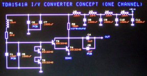
Designed it this afternoon, took me 5 minutes or so.
I attached concept schematics (quick screen shot from my CAD system).
Both T1 and T2 form a 1.2V reference voltage that matches (and tracks) 2 x Vbe of Darlington made up of T3 and T4. This Darlington circuit connects to the DAC output and forms a new external reference circuit (without output compliance) to drive the passive I/V resistor R2 (700 Ohm) generating as much amplitude as the +5V power supply will allow (up to approx. 4Vpp).
This 5V power supply (passive I/V resistor only) can be boosted to whatever practical voltage required to further increase ac amplitude.
Since the power amp uses GND for reference, and the I/V resistor uses +5V as reference, +5V power supply needs to be as clean as possible (I used 8th order LC low pass). I used a PCB bypass cap for achieving very low impedance between +5V and GND. This greatly enhances performance.
Man, you really try the opportunitys of the TDA1541A. Turning it backwards and inside out and back again
If modern chips would provide similar or better 44.1/16 playback quality I would use these for sure, saving me a lot of problems. But due to design flaws in these DAC chips it's not possible to achieve natural "live" sound quality, only "flat" clinical sound, and I don't like that, causes listening fatigue after an hour of listening.
Some of many reasons I stick with this ancient Philips chip is that it uses fast (low jitter) ECL / current steering logic (that's why this chip gets quite hot). It provides constant current output, and has very basic straight-forward construction (few components in the audio signal path, and few registers), allowing for very high dynamic resolution.
Since I am not convinced of high bit depth for playback (I do see advantages of the higher sample rates that go with it), and the vast majority of recordings are in 44.1/16, I plan to use 44.1/16 for now.
Do you really mean you can tap that amount of signal between the output and +5 V?
No, between external Darlington duplicate stage and +5V like I attempted to explain. Philips used almost exactly the same circuit inside the TDA1541A.
Do you care to share the inside schematics of TDA1541A? Where have you got that from?
Designed it this afternoon, took me 5 minutes or so.
I attached concept schematics (quick screen shot from my CAD system).
Both T1 and T2 form a 1.2V reference voltage that matches (and tracks) 2 x Vbe of Darlington made up of T3 and T4. This Darlington circuit connects to the DAC output and forms a new external reference circuit (without output compliance) to drive the passive I/V resistor R2 (700 Ohm) generating as much amplitude as the +5V power supply will allow (up to approx. 4Vpp).
This 5V power supply (passive I/V resistor only) can be boosted to whatever practical voltage required to further increase ac amplitude.
Since the power amp uses GND for reference, and the I/V resistor uses +5V as reference, +5V power supply needs to be as clean as possible (I used 8th order LC low pass). I used a PCB bypass cap for achieving very low impedance between +5V and GND. This greatly enhances performance.
Attachments
Last edited:
Hi Radioman62,
Since I am not convinced of high bit depth for playback (I do see advantages of the higher sample rates that go with it), and the vast majority of recordings are in 44.1/16, I plan to use 44.1/16 for now.
John, what is your critique of the PCM1704?
Thank you for your previous post. (#3137)
I understand perhaps half the things you commented (I discovered that I have to read and re-read your old posts because "it is all there") but it is clear to me that you are achieving the DAC wizard status
Do you have the complete internal schematics of the TDA1541???
Wouldn't it be nice to reproduce this DAC with discrete parts in the long rainy winter days? That way one could eliminate or attenuate the "annoying singularities" of it...
Enjoy,
M.
I understand perhaps half the things you commented (I discovered that I have to read and re-read your old posts because "it is all there") but it is clear to me that you are achieving the DAC wizard status
Do you have the complete internal schematics of the TDA1541???
Wouldn't it be nice to reproduce this DAC with discrete parts in the long rainy winter days?
That way one could eliminate or attenuate the "annoying singularities" of it...Enjoy,
M.
Hi Radioman62,
Since I am not convinced of high bit depth for playback (I do see advantages of the higher sample rates that go with it), and the vast majority of recordings are in 44.1/16, I plan to use 44.1/16 for now.
I agree 100%. The 65535 level combinations of 16 bit seems just fine. Your statement seems to be proven out by what that the Linear Interpolation DAC does in terms of reducing the amplitude of the false "step functions" every 22.6 uSecs. Reduce that energy spike at 22.6 uSecs and integrate it in smaller TIME increments works wonders for the signal.
Also why seemingly small jitter errors play such an important role. The time domain errors at work again.
The accumulative errors in the time domain have a much greater affect than the limitations of 16 bit resolution.
The resolution on the y axis 65535 steps (amplitude).... on the X axis 44.1k gives much less resolution if you assume 15K hz as the limit and even less for the harmonics....vs the resolution of the y axis.
I guess the trade offs for the original designers of CD Audio was the doubling the data for 98k sample or adding just a few more bits for 16 bit resolution....Then rely on "Capacitors" to integrate the signal in the time domain... YUCK, I hate capacitors...
So the 16 bits won out as still being able to fit enough music on the CD format. At the time in the late 70's and early 80's the cost of Improving on time resolution would have been prohibitive.
Time is always a very difficult thing to beat.... Once man wins the war against time, I think the Earth will be sucked up into a black hole...never to be seen from again....
....but time will win the battle ( ) Since we are are on topic of time... I think conventional speakers and other phase shift inducing devices (caps) are the enemy too.... More Time Domain errors added.
There is a huge Music store near me that sells CDs for 9$ US. Including the remastered versions that used to go for 20$ not so long ago. I am not sure how long this will last, but there are always people buying in that store. It is very hard to buy any CD quality online music when I can it for 9$ with the original packing. Old fashion yes.... I think time is the enemy of that store.
Just goes to prove that TIME IS MONEY......and that is just my 2 cents....
jk
Last edited:
Hi Maxlorenz,
Ehh, not a very good idea I guess. first problem you would encounter is getting a few thousand accurately matched transistors that also have perfect thermal tracking, and a very large breadboard of course. This already shows the next problem, the length of the wiring.
here is a link for downloading documents that describe DEM clock operation and show parts of internal chip schematics, interesting reading.
RapidShare: 1-CLICK Web hosting - Easy Filehosting
I couldn't attach the pdf files (too big)
Wouldn't it be nice to reproduce this DAC with discrete parts in the long rainy winter days? That way one could eliminate or attenuate the "annoying singularities" of it...
Ehh, not a very good idea I guess. first problem you would encounter is getting a few thousand accurately matched transistors that also have perfect thermal tracking, and a very large breadboard of course. This already shows the next problem, the length of the wiring.
here is a link for downloading documents that describe DEM clock operation and show parts of internal chip schematics, interesting reading.
RapidShare: 1-CLICK Web hosting - Easy Filehosting
I couldn't attach the pdf files (too big)

No, between external Darlington duplicate stage and +5V like I attempted to explain. Philips used almost exactly the same circuit inside the TDA1541A.
Designed it this afternoon, took me 5 minutes or so.
I attached concept schematics (quick screen shot from my CAD system).
Sorry for that one
 . I have re-read and your latest comments also made it more clear. Thank you for the exhaustive explenation.
Thanks to you there are now many angles to try with this old chip.
You may also have doubled the price on TDA1541A at Ebay, those few years you have been at DIY Audio.

At the SD-card player thread i wrote a little review of the new EC-designs TDA1543 DAC. I own the DAC now over 2 weeks. More and more happy -and impressed- with it. the DAC is implemented in a application with a Squeezebox reciever. I feed the DAC with a Batterie>Thell regulator. Tried various tweaks last week and noticed that this DAC, like other TDA1543 implementations, is very, very sensitive for Data and/or PS noise. Even with John's extended approach to get every signal clean to the chip is not a guaranty for perfect sound when fitted the DAC in a other application then the SD-card player. Groundnoise is a culprit. Even the way of LAN connection to the SB is affecting the sound. Got it all optimized now (as far as i could) The level of details, the tonality and timbre are stunning. The audible detail-level approaches OS details. I can listen again to Patricia Barbers excellent recordings without being aware of missing details. Never thought that would be possible with a single TDA1543.
Dear -EC-,
Thanks for #3146.
I suspected that. It would be ment as part of my electronics education
The file is still dowloading...
Maybe I should build first a discrete TDA1543
Thanks for #3146.
Ehh, not a very good idea I guess. first problem you would encounter is getting a few thousand accurately matched transistors that also have perfect thermal tracking, and a very large breadboard of course. This already shows the next problem, the length of the wiring.
I suspected that. It would be ment as part of my electronics education
The file is still dowloading...
Maybe I should build first a discrete TDA1543
After a quick read of the docs provided....
Would the DEM clocking of the 6 MSBs be a form of Oversampling?
jk
Would the DEM clocking of the 6 MSBs be a form of Oversampling?
jk
Hi Maxlorenz,
Ehh, not a very good idea I guess. first problem you would encounter is getting a few thousand accurately matched transistors that also have perfect thermal tracking, and a very large breadboard of course. This already shows the next problem, the length of the wiring.
here is a link for downloading documents that describe DEM clock operation and show parts of internal chip schematics, interesting reading.
RapidShare: 1-CLICK Web hosting - Easy Filehosting
I couldn't attach the pdf files (too big)
Is there any Information about the internal on chip schematics of AD1862? It is a multibit DAC from the same era.
I plan to build a new DAC with this IC. If there were any information about internals, I could plan an equivalent to the IIS Attenuator.
20 bit resolution would be interesting for the SD Card player too. The additional 4 bit would allow for a digital volume control within some range and for playing 24/96 material with 20 bit resolution, which should be enough ;-)
Does someone know a good source for the AD1862?
Hi.I got a Tda1541a chip today.I want to build a Nos dac with one tda1541.I want to have high output.5-6volts RMS.I have 2sj74bl and 2sk170bl and V grades.I also have 2sc2240/sa970bl.I will buy Elna silmic2 capacitors.Do you prefer a good schematic? I want to build a high end circuit.
noWould the DEM clocking of the 6 MSBs be a form of Oversampling?
Hi umut1001,
Use schematics (post #3142), requires 4 x 2SC2240 / channel.
6V rms equals 6 * sqrt(2) * 2 = 16.97Vpp.
I/V resistor value needs to be r = v / i, r = 17 / 0.004 = 4K25. I/V resistor power supply (not 5V TDA1541A power supply!) must then be increased to approx. 20V DC. You might use a JFET unity gain buffer (2SJ74 / 2SK170) to buffer voltage across passive 4k25 I/V resistor.
Good TDA1541A application can.
Hi.I got a Tda1541a chip today.I want to build a Nos dac with one tda1541.I want to have high output.5-6volts RMS.I have 2sj74bl and 2sk170bl and V grades.I also have 2sc2240/sa970bl.I will buy Elna silmic2 capacitors.Do you prefer a good schematic? I want to build a high end circuit.
Use schematics (post #3142), requires 4 x 2SC2240 / channel.
6V rms equals 6 * sqrt(2) * 2 = 16.97Vpp.
I/V resistor value needs to be r = v / i, r = 17 / 0.004 = 4K25. I/V resistor power supply (not 5V TDA1541A power supply!) must then be increased to approx. 20V DC. You might use a JFET unity gain buffer (2SJ74 / 2SK170) to buffer voltage across passive 4k25 I/V resistor.
I am curious that tda1541 can play better than my emu card
Good TDA1541A application can.
Hi omainik,
AD1862 uses CMOS logic elements, and has no current steering / ECL like TDA154x. TDA154x I2S attenuator (200mVpp output) does not work here.
I explained in the "Lossless SD-player thread" why I don't want to use high res formats for the SD-transport.
Is there any Information about the internal on chip schematics of AD1862? It is a multibit DAC from the same era.
I plan to build a new DAC with this IC. If there were any information about internals, I could plan an equivalent to the IIS Attenuator.
AD1862 uses CMOS logic elements, and has no current steering / ECL like TDA154x. TDA154x I2S attenuator (200mVpp output) does not work here.
20 bit resolution would be interesting for the SD Card player too. The additional 4 bit would allow for a digital volume control within some range and for playing 24/96 material with 20 bit resolution, which should be enough ;-)
I explained in the "Lossless SD-player thread" why I don't want to use high res formats for the SD-transport.
Hi jstang,
DEM means Dynamic Element Matching, or in other words a continuous calibration system (6 MSBs). This means that component tolerances in the passive current dividers for the 6 MSBs are continuoulsy corrected using the DEM technique. Passive current dividers with the extra DEM correction circuit are called active dividers since they have active correction circuit (DEM circuit) placed after the passive current divider.
TDA154x chips derive all binary weighted output currents from a single current reference source. This is done by splitting-up this current in smaller currents, using current dividers. This provides 16, binary weighted constant current outputs. In case of TDA1541A this would look like this:
Bit15, DEM, (MSB), 2mA
Bit14, DEM, 1mA
Bit13, DEM, 0.5mA
Bit12, DEM, 250uAmA
Bit11, DEM, 125uA
Bit10, DEM, 62.5uA
Bit9, 31.25mA
Bit8, 15.625uA
Bit7, 7.8125uA
Bit6, 3.90625uA
Bit5, 1.953125uA
Bit4, 976.5625nA
Bit3, 488.28125nA
Bit2, 244.140625nA
Bit1, 122.070313nA
Bit0, (LSB) 61.035156nA
Note how low the LSB current is, only 61 nano amperes! LSBs can easily drop below system noise level when power supplies aren't super clean, and output circuit fails to maintain extreme low noise levels. And this is "only" 16 bit resolution. Imagine how critical 20 or even 24 bit systems will get. Using above current division, LSB in a 24 bit system would translate to 238pA!
The analogue constant output current is generated by combining required constant bit currents from the active (6) and passive (10) current divider outputs. This in turn is determined by the sample value (0-65535) received trough the I2S interface.
When selecting Philips I2S format (pin 27 tied to +5V), TDA1541A first clocks in L(WS=0) and R(WS=1) DATA. After receiving serial data for both channels in the input register, data is latched into the output register on the first positive going edge of BCK, after WS has gone back to zero.
So BCK determines the exact moment the output latch data (and derived DAC output current) changes. therefore BCK needs to have lowest jitter.
After a quick read of the docs provided....
Would the DEM clocking of the 6 MSBs be a form of Oversampling?
DEM means Dynamic Element Matching, or in other words a continuous calibration system (6 MSBs). This means that component tolerances in the passive current dividers for the 6 MSBs are continuoulsy corrected using the DEM technique. Passive current dividers with the extra DEM correction circuit are called active dividers since they have active correction circuit (DEM circuit) placed after the passive current divider.
TDA154x chips derive all binary weighted output currents from a single current reference source. This is done by splitting-up this current in smaller currents, using current dividers. This provides 16, binary weighted constant current outputs. In case of TDA1541A this would look like this:
Bit15, DEM, (MSB), 2mA
Bit14, DEM, 1mA
Bit13, DEM, 0.5mA
Bit12, DEM, 250uAmA
Bit11, DEM, 125uA
Bit10, DEM, 62.5uA
Bit9, 31.25mA
Bit8, 15.625uA
Bit7, 7.8125uA
Bit6, 3.90625uA
Bit5, 1.953125uA
Bit4, 976.5625nA
Bit3, 488.28125nA
Bit2, 244.140625nA
Bit1, 122.070313nA
Bit0, (LSB) 61.035156nA
Note how low the LSB current is, only 61 nano amperes! LSBs can easily drop below system noise level when power supplies aren't super clean, and output circuit fails to maintain extreme low noise levels. And this is "only" 16 bit resolution. Imagine how critical 20 or even 24 bit systems will get. Using above current division, LSB in a 24 bit system would translate to 238pA!
The analogue constant output current is generated by combining required constant bit currents from the active (6) and passive (10) current divider outputs. This in turn is determined by the sample value (0-65535) received trough the I2S interface.
When selecting Philips I2S format (pin 27 tied to +5V), TDA1541A first clocks in L(WS=0) and R(WS=1) DATA. After receiving serial data for both channels in the input register, data is latched into the output register on the first positive going edge of BCK, after WS has gone back to zero.
So BCK determines the exact moment the output latch data (and derived DAC output current) changes. therefore BCK needs to have lowest jitter.
- Home
- Source & Line
- Digital Line Level
- Building the ultimate NOS DAC using TDA1541A