If i get this right, this makes every sinewave longer !? Infact this reduce the frequens, and make the sound "false" from the original signal. Of course no existing person in the world can hear this.
??

I hope that wasn't a comment about my statement? I did not talk about changed frequency. Just the amplitude of the output signal gone trough a resistor. Your interpolation discussing doesn't apply to what I told you above.
It's the available voltage who sets the maximum roof where the DAC clips the signal. If you raise output so you push more current then you have to half the resistor for every doubling of DAC. You must not go in to that voltage roof which corresponds to max 80 - 90mV RMS.
But that You may allready know I hope
I'm only refering to practical tests which shows that this DAC distorts the audio signal if you have to large resistor.
Look here
Vet inte hur den här tråden kunde hamna här, den var ämnad till en tråd runt 3-8 nånsans.??
I hope that wasn't a comment about my statement? I did not talk about changed frequency. Just the amplitude of the output signal gone trough a resistor. Your interpolation discussing doesn't apply to what I told you above.
It's the available voltage who sets the maximum roof where the DAC clips the signal. If you raise output so you push more current then you have to half the resistor for every doubling of DAC. You must not go in to that voltage roof which corresponds to max 80 - 90mV RMS.
But that You may allready know I hope
I'm only refering to practical tests which shows that this DAC distorts the audio signal if you have to large resistor.
Look here
17bit ???
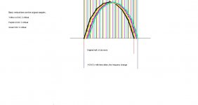
First i will tell i'm new in diy, and i really like this thread with the TDA1541A DAC chip. I thinking in this, so i can not sleep or work. please someone, tell me if ai'm totally wrong or right in this. Yes, i can see on the osilloscope that this really improve the signal, but what i don't understand is ... All the DAC's working with 16bit resolution and i have hard to belive that with 4 DAC's it should bee 17bit. I see this impossible. Because the only thing don is to move the signal in time, and make it's "dots" in diffrent levels of the 3 extra samples. But, the sine wave is just moved in time, and dischaped from original,wouldn't paralell be better? The extra samples are just virtuals and not in phase with the originall sample. To make it be in phase something have to be don with the signal after leaving the DAC's. How it looks like this on the osilloscope i have no idea, but for sure i will build one of these. Exelent work !!!! I send a picture to explain how i think.
First i will tell i'm new in diy, and i really like this thread with the TDA1541A DAC chip. I thinking in this, so i can not sleep or work. please someone, tell me if ai'm totally wrong or right in this. Yes, i can see on the osilloscope that this really improve the signal, but what i don't understand is ... All the DAC's working with 16bit resolution and i have hard to belive that with 4 DAC's it should bee 17bit. I see this impossible. Because the only thing don is to move the signal in time, and make it's "dots" in diffrent levels of the 3 extra samples. But, the sine wave is just moved in time, and dischaped from original,wouldn't paralell be better? The extra samples are just virtuals and not in phase with the originall sample. To make it be in phase something have to be don with the signal after leaving the DAC's. How it looks like this on the osilloscope i have no idea, but for sure i will build one of these. Exelent work !!!! I send a picture to explain how i think.
Attachments
Vet inte hur den här tråden kunde hamna här, den var ämnad till en tråd runt 3-8 nånsans.
Welcome fragglan
You have to quote a post if it's that far away. Particulary if it's an answer or reflection over a post from the first page of this thread, soon 4 years ago.
PS Audio Perfect Wave Transport/DAC
Hi EC, been a while since I last saw your post. I see that you are trying to build an integrated lossless SD memory player/DAC now. It seems like your project is very similar to PS Audio PW Transport/DAC. It uses SD memory to store the digital data from either CD or high resolution DVD (or hard drive if you choose to use DAC only with its Network Bridge Card that is soon to be released). The Transport collects the data and strips all timining info and reclocks it in SD memory before sending it off to its DAC (WAV format currently) via I2S interface using their proprietary I2S HDMI interface. The DAC uses the latest Wolfson chip that has built in apodizing filters. Interestingly it has a "Native" mode where ASR converter is bypassed (ie, non oversampling). You can hook the DAC directly to the amp because it has its own digital volume control. According to PS Audio, you don't lose resolution on redbook CD if you play it above 50% of max volume. I understand the analogue output stage on the DAC is discrete without opamps. Have you seen or heard it?
Hi EC, been a while since I last saw your post. I see that you are trying to build an integrated lossless SD memory player/DAC now. It seems like your project is very similar to PS Audio PW Transport/DAC. It uses SD memory to store the digital data from either CD or high resolution DVD (or hard drive if you choose to use DAC only with its Network Bridge Card that is soon to be released). The Transport collects the data and strips all timining info and reclocks it in SD memory before sending it off to its DAC (WAV format currently) via I2S interface using their proprietary I2S HDMI interface. The DAC uses the latest Wolfson chip that has built in apodizing filters. Interestingly it has a "Native" mode where ASR converter is bypassed (ie, non oversampling). You can hook the DAC directly to the amp because it has its own digital volume control. According to PS Audio, you don't lose resolution on redbook CD if you play it above 50% of max volume. I understand the analogue output stage on the DAC is discrete without opamps. Have you seen or heard it?
Why continue to use the TDA1541 and not start a new project like this with AD1865 or AD1862 ?
DAC End 2 - the AD1865N-K with single ended vacuum output stage
http://www.diyaudio.com/forums/group-buys/155960-dac-end-andrea-ciuffoli-group-buys.html
DAC End 2 - the AD1865N-K with single ended vacuum output stage
http://www.diyaudio.com/forums/group-buys/155960-dac-end-andrea-ciuffoli-group-buys.html
Why continue to use the TDA1541 and not start a new project like this with AD1865 or AD1862 ?
DAC End 2 - the AD1865N-K with single ended vacuum output stage
http://www.diyaudio.com/forums/group-buys/155960-dac-end-andrea-ciuffoli-group-buys.html
AN1865N-K is easy to find now
Another D1M DAC.
This is my other D1M USB NOS DAC:
Picasa Web Albums - mauricio
It has "floating charge-transfer supply" and the new SuperTeddyRegs for the DAC chip module and for the transimpedance amplifier. This uses a variable R, provided by a resistor based potentiometer, with a good quality (low tempco) resistor in parallel. This mod allows for direct connection to the power amps (who wants preamps? Puaggh). Output caps are NOS (new old stock) Russian PEPT.
-ECdesigns'- USB receiver is powered AND isolated from laptop through the ADUM4160 module (not in the photo).
adum4160 « Circuits@Home
Now I have to try LED voltage references...and the I2S attenuators...
I am using here and there some chokes to evaluate their effect.
Cheers,
M
Last edited:
Thanks John (ECdesign..)
Ok just finished my conversion to linear Interpolation on my 4X TDA1541 ..... WOW.... WOW .... WOW...
Listening to Van Halen Eruption now .... did I say WOW....
I turned on each DAC one at a time...and the music came alive with each DAC added. It added depth, layering and separation of the details & removed the digital edginess. FYI, The rest of my system is Vintage 70's Marantz, 7t + Model 500 and Ohm Fs. The Transport is a CD-Pro.
johnk
Last edited:
Hi jstang,
I had that experience during development of the DI8 DAC.
But now, the ISD player makes the DI8 and DI4 (4 x TDA1541A-S1) sound like plain CD players by comparison. So what you are experiencing with the DI DAC is only the tip of the iceberg.
I would say that the DI8 sounds impressive, and the ISD player sounds highly transparent, detailed, fast, natural and very refined. Musical instruments sound natural, pure, and there is lots of "air" around the instruments.
Due to very low noise levels, background is pitch black. This enables accurate reproduction of both recording noise (spectrum) and micro details that are often buried in this noise. Every recording contains noise, when this is not audible on your set, the micro details of similar amplitude will be gone as well.
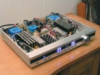
I attached a photograph of this Integrated SD Player. It's a complete super-tuned audio set in one compact box, SD-memory card in (up to 52 lossless CDs on a single 32Gb card), speaker out.
This is the result of 2 years of intensive research and endless listening tests. It's loaded with tricks and innovations. It merges both NOS DAC and SD-player projects.
Starting at the source, this is a solid-state player, tuned for minimum noise and interference levels, outputting 32 bits / frame I2S, providing lowest possible bit clock (lowest DAC on-chip ground-bounce levels, lowest on-chip timing jitter). Display consists of two large white 7-segments displays that offer excellent readability.
The source drives the TDA1543 DAC module, this is no ordinary TDA1543 application, this is a super-tuned application with separate Vref voltages for L and R channels, using 20th order LC filters. I had to make the I/V resistors myself as I couldn't find a suitable audiophile resistor for this application. The TDA1543 has I2S attenuators (200mVpp signal level) and a unique dynamic jitter attenuator circuit for BCK.
Both source and DAC chip are driven from a 11.2896 MHz superclock with integrated synchronous reclocker. This is the only clock in this system. The superclock power supply is also filtered by a 20th order LC filter for achieving extreme performance levels. The synchronous reclocker is driven through a capacitive node, providing galvanic insulation between clock and reclocker. The recloker receives a filtered clock signal (has passed a 3-crystal filter) offering high spectral purity.
Since I wasn't able to find suitable audiophile coupling caps yet, I also had to make these myself (modules left and right from the DAC module). These are very high speed hybrid caps.
The signal is then attenuated (pot) and passed to the only active part in the signal path (bridge power amps). These amps have balanced inputs, and outputs. I tap the GND reference straight from the I/V resistor.
The bridge power amps (left and right) are fully DC-coupled, have no global feedback, and super tuned for maximum dynamic resolution.
They use two dual JFETs and 4 power MOSFETs, that's all. They have large on-board reservoir caps (60,000uF) that can provide instant peak currents. The power amps have on-board mains power supplies using unique stepped rectifiers, offering better refinement when running on mains voltage. These amps were designed to remain completely stable, far into the MHz range (ISD player uses large bandwidth signal processing in order to achieve highest possible dynamic resolution).
The main power supply (center rear) consists of a transformer, 3-stage stepped rectifiers, 2 discrete series-cascaded regulators (filtered LED reference for lowest noise levels), and 4th order LC filters on each output. All voltages track, so minor (LF) fluctuations are common for all connected loads. One single transformer also injects far less mains noise compared to multiple-transformer power supplies.
The ISD player can be operated locally (keys, volume knob) or by remote control.
Since one SD(HC) card can hold up to 52 CDs at the moment, the ISD player is basically a 52 CD changer as well. It also has random disc / track function, so you can listen to your favorite music (play lists) all day without touching the unit. SD(HC) card of 32Gb capacity offers approx. 52 hours of non-stop high-performance digital audio playback.
Since this is a solid-state player, it's dead quiet (no moving parts). It's also far less sensitive to external mechanical vibration.
How to get your favorite music on a SD-card? I offer a free application for mac, linux and windows that reads play lists, converts them into WAV (if required) and writes them to the SD-card using correct directory and file names at the push of a key. leaflets with (for reference) can be printed too.
The ISD player modules are available separately for use in other projects, or to build an ISD player step by step.
Since the concept is fully modular, different DAC modules could be used in the future. TDA1541A DAC module is already planned, but first I need to be able to outperform super-tuned TDA1543 application, not an easy task as the TDA1541A probably requires an active output circuit.
The TDA1543 DAC module has fully passive output, so active output stage distortion is completely eliminated.
I had that experience during development of the DI8 DAC.
But now, the ISD player makes the DI8 and DI4 (4 x TDA1541A-S1) sound like plain CD players by comparison. So what you are experiencing with the DI DAC is only the tip of the iceberg.
I would say that the DI8 sounds impressive, and the ISD player sounds highly transparent, detailed, fast, natural and very refined. Musical instruments sound natural, pure, and there is lots of "air" around the instruments.
Due to very low noise levels, background is pitch black. This enables accurate reproduction of both recording noise (spectrum) and micro details that are often buried in this noise. Every recording contains noise, when this is not audible on your set, the micro details of similar amplitude will be gone as well.
I attached a photograph of this Integrated SD Player. It's a complete super-tuned audio set in one compact box, SD-memory card in (up to 52 lossless CDs on a single 32Gb card), speaker out.
This is the result of 2 years of intensive research and endless listening tests. It's loaded with tricks and innovations. It merges both NOS DAC and SD-player projects.
Starting at the source, this is a solid-state player, tuned for minimum noise and interference levels, outputting 32 bits / frame I2S, providing lowest possible bit clock (lowest DAC on-chip ground-bounce levels, lowest on-chip timing jitter). Display consists of two large white 7-segments displays that offer excellent readability.
The source drives the TDA1543 DAC module, this is no ordinary TDA1543 application, this is a super-tuned application with separate Vref voltages for L and R channels, using 20th order LC filters. I had to make the I/V resistors myself as I couldn't find a suitable audiophile resistor for this application. The TDA1543 has I2S attenuators (200mVpp signal level) and a unique dynamic jitter attenuator circuit for BCK.
Both source and DAC chip are driven from a 11.2896 MHz superclock with integrated synchronous reclocker. This is the only clock in this system. The superclock power supply is also filtered by a 20th order LC filter for achieving extreme performance levels. The synchronous reclocker is driven through a capacitive node, providing galvanic insulation between clock and reclocker. The recloker receives a filtered clock signal (has passed a 3-crystal filter) offering high spectral purity.
Since I wasn't able to find suitable audiophile coupling caps yet, I also had to make these myself (modules left and right from the DAC module). These are very high speed hybrid caps.
The signal is then attenuated (pot) and passed to the only active part in the signal path (bridge power amps). These amps have balanced inputs, and outputs. I tap the GND reference straight from the I/V resistor.
The bridge power amps (left and right) are fully DC-coupled, have no global feedback, and super tuned for maximum dynamic resolution.
They use two dual JFETs and 4 power MOSFETs, that's all. They have large on-board reservoir caps (60,000uF) that can provide instant peak currents. The power amps have on-board mains power supplies using unique stepped rectifiers, offering better refinement when running on mains voltage. These amps were designed to remain completely stable, far into the MHz range (ISD player uses large bandwidth signal processing in order to achieve highest possible dynamic resolution).
The main power supply (center rear) consists of a transformer, 3-stage stepped rectifiers, 2 discrete series-cascaded regulators (filtered LED reference for lowest noise levels), and 4th order LC filters on each output. All voltages track, so minor (LF) fluctuations are common for all connected loads. One single transformer also injects far less mains noise compared to multiple-transformer power supplies.
The ISD player can be operated locally (keys, volume knob) or by remote control.
Since one SD(HC) card can hold up to 52 CDs at the moment, the ISD player is basically a 52 CD changer as well. It also has random disc / track function, so you can listen to your favorite music (play lists) all day without touching the unit. SD(HC) card of 32Gb capacity offers approx. 52 hours of non-stop high-performance digital audio playback.
Since this is a solid-state player, it's dead quiet (no moving parts). It's also far less sensitive to external mechanical vibration.
How to get your favorite music on a SD-card? I offer a free application for mac, linux and windows that reads play lists, converts them into WAV (if required) and writes them to the SD-card using correct directory and file names at the push of a key. leaflets with (for reference) can be printed too.
The ISD player modules are available separately for use in other projects, or to build an ISD player step by step.
Since the concept is fully modular, different DAC modules could be used in the future. TDA1541A DAC module is already planned, but first I need to be able to outperform super-tuned TDA1543 application, not an easy task as the TDA1541A probably requires an active output circuit.
The TDA1543 DAC module has fully passive output, so active output stage distortion is completely eliminated.
Attachments
Hi jstang,
I had that experience during development of the DI8 DAC.
But now, the ISD player makes the DI8 and DI4 (4 x TDA1541A-S1) sound like plain CD players by comparison. So what you are experiencing with the DI DAC is only the tip of the iceberg.
Oh no....
Here I go again.... Heck it keeps me out of trouble.... johnk
Yes congrats, John
Is the clock module a drop in replacement for 11.289MHz clock or is there some tweaking to do to it for different DACs - what are the parameters that optimise it's value in the system i.e you've done a lot of special treatment of the clock with regard to reducing signal levels, etc. do these only have real value when implemented with your TDA1543 DAC?
Is the clock module a drop in replacement for 11.289MHz clock or is there some tweaking to do to it for different DACs - what are the parameters that optimise it's value in the system i.e you've done a lot of special treatment of the clock with regard to reducing signal levels, etc. do these only have real value when implemented with your TDA1543 DAC?
Hi jkeny,
The 11.2896 Mhz superclock has an integrated reclocker that's fed by the filtered oscillator signal through a capacitive node. This reclocker, and especially the way it's driven, determines performance.
The superclock also has a 11.2896 MHz buffered output (discrete complementary JFET clock buffer) that can be used to slave the source. I use a 1 K Ohm damping resistor between superclock output and SD-transport, same resistor value can be used to clock the squeezebox.
I used a dynamic jitter attenuator that drives the TDA154x BCK input (1.2V DC bias, 200mVpp signal amplitude), output impedance of the dynamic jitter attenuator equals approx. 100 Ohms. The DC bias voltage is extracted from the BCK input signal. If DAC chips won't accept low amplitude signals, ground-bounce in the on-chip I2S input circuit will be significantly increased, causing increased on-chip jitter and crosstalk to analogue outputs. The current steering logic is a big advantage of the TDA154x series.
This superclock needs an extremely clean power supply, so forget about the conventional 780x, TL431, and LM317 regulators.
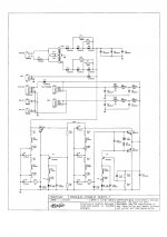
I attached a concept schematic of the ISD player logic power supply that also feeds the superclock through an additional 20th order LC filter.
Rectifier is the novel stepped rectifier (3-stage version used here).
Pre-regulator uses a filtered LED reference, and base drive voltage first passes a 6th order LC filter that also acts as capacitance multiplier.
The post regulator also uses a filtered LED reference and 6th order LC filter to clean the base drive voltage. It has a complementary output.
The 5.4V post regulator output then passes 4th order LC filters for SD-transport and DAC module.
Is the clock module a drop in replacement for 11.289MHz clock or is there some tweaking to do to it for different DACs - what are the parameters that optimise it's value in the system i.e you've done a lot of special treatment of the clock with regard to reducing signal levels, etc. do these only have real value when implemented with your TDA1543 DAC?
The 11.2896 Mhz superclock has an integrated reclocker that's fed by the filtered oscillator signal through a capacitive node. This reclocker, and especially the way it's driven, determines performance.
The superclock also has a 11.2896 MHz buffered output (discrete complementary JFET clock buffer) that can be used to slave the source. I use a 1 K Ohm damping resistor between superclock output and SD-transport, same resistor value can be used to clock the squeezebox.
I used a dynamic jitter attenuator that drives the TDA154x BCK input (1.2V DC bias, 200mVpp signal amplitude), output impedance of the dynamic jitter attenuator equals approx. 100 Ohms. The DC bias voltage is extracted from the BCK input signal. If DAC chips won't accept low amplitude signals, ground-bounce in the on-chip I2S input circuit will be significantly increased, causing increased on-chip jitter and crosstalk to analogue outputs. The current steering logic is a big advantage of the TDA154x series.
This superclock needs an extremely clean power supply, so forget about the conventional 780x, TL431, and LM317 regulators.
I attached a concept schematic of the ISD player logic power supply that also feeds the superclock through an additional 20th order LC filter.
Rectifier is the novel stepped rectifier (3-stage version used here).
Pre-regulator uses a filtered LED reference, and base drive voltage first passes a 6th order LC filter that also acts as capacitance multiplier.
The post regulator also uses a filtered LED reference and 6th order LC filter to clean the base drive voltage. It has a complementary output.
The 5.4V post regulator output then passes 4th order LC filters for SD-transport and DAC module.
Attachments
Hi jstang,
Since I wasn't able to find suitable audiophile coupling caps yet, I also had to make these myself (modules left and right from the DAC module). These are very high speed hybrid caps.
John those caps are very interesting... Do you plan to sell them? How can I build them? Any URLs?
thanks,
Johnk
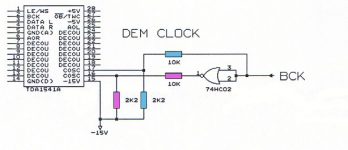
I attached latest DEM clock and I2S attenuator schematics. The I2S attenuators can also be used for the TDA1543.
The DEM clock circuit consists of two resistive attenuators that perform biasing, level-shifting and attenuation. The DEM clock frequency has been increased to 2.8224 MHz (bit clock).
The I2S attenuators provide both a bias voltage (approx. 1.2V), and attenuation of the I2S signals. By lowering I2S signal amplitude, sound get's much more refined, due to reduction of I2S interference.
The bit clock (BCK) attenuator needs a choke (10mH Panasonic ferrite-core choke) to attenuate power supply noise. This choke will also provide a high impedance to +5V, so the series resistor value can be increased, and the shunt resistor value can be lowered.
I used multiple 100R resistors in order to minimize the effect of resistor stray capacitance.
I tried many, more complicated discrete designs. This simple circuit performs best so far, especially when using multiple low noise transistors in parallel, minimizing current flow through each transistor.
The simple trans-impedance I/V converter uses current steering and is extremely fast (large bandwidth). By using few high quality (low noise) parts, signal degradation can be minimized.
Single-ended output (class A) seems to provide cleanest sound, as cross-over distortion is eliminated.
@ ecdesigns
First of all
 for your great work arround the 1541A !
Do you think it will be a problem to insert your latest DEM reclock on my new TDA1541A Module ?
Regards to the Netherlands,
Oliver
Attachments
Hi jstang,
It's basically a Monacor 3.3uF MKT capacitor with a bypass cap made from a euro sized (100 x 160mm) double-sided 0.5mm thick PCB (epoxy) material. because the PCB was rather large, I cut it into 4 pieces and milled / drilled them to form a compact capacitor.
The Monacor cap is inside the packet, mounted on a single-sided PCB with a slot for the capacitor. The PCB material was arranged so I have "outer foil" on top and bottom for screening. The parts aren't very expensive (approx $8 for one cap), but I spent over an hour milling, tinning and assembling these hybrid caps.
It's also very important to check for short circuits and use fine sandpaper to smoothen the PCB edges, removing possible short circuits. If the package has been assembled and you measure a short circuit you have a big problem.
Why on earth use a double-sided PCB as bypass cap?
The copper foils are fused to the epoxy base material (no air pockets). The PCB (enforced with glass fiber) is way more stable than any foil. In other words, this cap has less mechanical resonance compared to a very thin flexible foil.
Bypass caps only work effectively if they have very low self resonance, otherwise you simply add resonances from both, main and bypass cap, making matters worse. This is the main reason why bypass caps usually aren't very effective.
The bypass cap value does not have to be that big, the PCB bypass cap value equals approx. 1.5nF, this is sufficient for a 3.3uF main cap.
The idea is to dampen the main cap resonances, creating better specs than when using only a single (flawed) cap. This $8 coupling cap was directly compared with a V-cap TFTF (switch), and all people who listened to both caps preferred the $8 cap without knowing what cap was selected. The V-cap TFTF is regarded as one of the better audiophile caps and a single 3uF version cost around $699. The V-cap TFTF performance didn't improve significantly when bypassed with a PCB.
Capacitor test link:
The Great Capacitor Shoot-Out
I wasn't able to test Duelund VSF copper foil caps, still no caps, after almost 3 months! waiting and paying in advance. I ordered them from "De Audiofabriek" an official Dutch Duelund dealer.
I used similar hybrid caps in my SR60 passive crossover. Here I had an extra problem, the power that needed to be handled by the caps would for sure cause unacceptable resonances. I ended up using 4 ... 5 capacitors in series / parallel configuration using a mix of tin foil and polypropylene plus caps from Intertechnik, all bypassed by a PCB cap. The idea was to spread the power across multiple caps, thereby reducing cap resonances as each cap now receives less power. The remaining resonances are then dampened by the PCB bypass cap. When using multiple caps, it's possible to mix specific properties of different cap types. Tin foils sound very clean but "thin", ideal for tweeters, not for midrange. Polypropylene lacks tin foil clarity, but has better midrange performance, both caps combined create a new cap with better performance.
I also make connections as close to the capacitor housing as possible, preferably using flat conductors like PCB material.
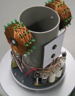
I attached a photograph of the SR60 high resolution passive crossover (2-way) using 2 hybrid caps and PCB bypass cap.
John those caps are very interesting... Do you plan to sell them? How can I build them? Any URLs?
It's basically a Monacor 3.3uF MKT capacitor with a bypass cap made from a euro sized (100 x 160mm) double-sided 0.5mm thick PCB (epoxy) material. because the PCB was rather large, I cut it into 4 pieces and milled / drilled them to form a compact capacitor.
The Monacor cap is inside the packet, mounted on a single-sided PCB with a slot for the capacitor. The PCB material was arranged so I have "outer foil" on top and bottom for screening. The parts aren't very expensive (approx $8 for one cap), but I spent over an hour milling, tinning and assembling these hybrid caps.
It's also very important to check for short circuits and use fine sandpaper to smoothen the PCB edges, removing possible short circuits. If the package has been assembled and you measure a short circuit you have a big problem.
Why on earth use a double-sided PCB as bypass cap?
The copper foils are fused to the epoxy base material (no air pockets). The PCB (enforced with glass fiber) is way more stable than any foil. In other words, this cap has less mechanical resonance compared to a very thin flexible foil.
Bypass caps only work effectively if they have very low self resonance, otherwise you simply add resonances from both, main and bypass cap, making matters worse. This is the main reason why bypass caps usually aren't very effective.
The bypass cap value does not have to be that big, the PCB bypass cap value equals approx. 1.5nF, this is sufficient for a 3.3uF main cap.
The idea is to dampen the main cap resonances, creating better specs than when using only a single (flawed) cap. This $8 coupling cap was directly compared with a V-cap TFTF (switch), and all people who listened to both caps preferred the $8 cap without knowing what cap was selected. The V-cap TFTF is regarded as one of the better audiophile caps and a single 3uF version cost around $699. The V-cap TFTF performance didn't improve significantly when bypassed with a PCB.
Capacitor test link:
The Great Capacitor Shoot-Out
I wasn't able to test Duelund VSF copper foil caps, still no caps, after almost 3 months! waiting and paying in advance. I ordered them from "De Audiofabriek" an official Dutch Duelund dealer.
I used similar hybrid caps in my SR60 passive crossover. Here I had an extra problem, the power that needed to be handled by the caps would for sure cause unacceptable resonances. I ended up using 4 ... 5 capacitors in series / parallel configuration using a mix of tin foil and polypropylene plus caps from Intertechnik, all bypassed by a PCB cap. The idea was to spread the power across multiple caps, thereby reducing cap resonances as each cap now receives less power. The remaining resonances are then dampened by the PCB bypass cap. When using multiple caps, it's possible to mix specific properties of different cap types. Tin foils sound very clean but "thin", ideal for tweeters, not for midrange. Polypropylene lacks tin foil clarity, but has better midrange performance, both caps combined create a new cap with better performance.
I also make connections as close to the capacitor housing as possible, preferably using flat conductors like PCB material.
I attached a photograph of the SR60 high resolution passive crossover (2-way) using 2 hybrid caps and PCB bypass cap.
Attachments
Dear EC,
Again, congratulations for your amazing job, researching and creating such unconventional answers to common problems.
Two questions:
Can we use the stepped rectifier approach on your own charge-transfer supply?
I mean, probably after the Darlington/Mosfet active device?
I understand your DIY caps are those shining sandwich-like structures, one at each side of the DAC PCB...if so, have you tried damping them with wood? ("Guttemberg style caps" ).
Cheers,
M.
Again, congratulations for your amazing job, researching and creating such unconventional answers to common problems.
Two questions:
Can we use the stepped rectifier approach on your own charge-transfer supply?
I mean, probably after the Darlington/Mosfet active device?
I understand your DIY caps are those shining sandwich-like structures, one at each side of the DAC PCB...if so, have you tried damping them with wood?
("Guttemberg style caps" ).Cheers,
M.
Whats the Voltage rating of such a PCB based cap? About 5000V ?
Not that I am really concerned about it...I think it would survive my tube output.
Too bad I am out of space in my chassis....otherwise this would be a project for this weekend. Hmmmm, Time for a new chassis ?
Thanks much!
jk
Not that I am really concerned about it...I think it would survive my tube output.
Too bad I am out of space in my chassis....otherwise this would be a project for this weekend. Hmmmm, Time for a new chassis ?
Thanks much!
jk
Hi jstang,
Why on earth use a double-sided PCB as bypass cap?
Hi maxlorenz,
Yes, this is possible, but the stepped rectifier should connect directly to the transformer, it requires an ac voltage to function. The function of the stepped rectifier is reducing peak current (when the diode suddenly starts conducting) and possible back-emf (when the diode suddenly stops conducting). This is done by increasing / decreasing reservoir cap charge current step wise. The audible result is a cleaner more refined sound. It works especially well with power amp supplies where large charge currents are to be expected.
Yes those are the coupling caps. The main capacitor (that's sensitive to vibration) can be mounted in damping material, or the complete module can be mounted on dampers, using module mass for more effective damping.
Can we use the stepped rectifier approach on your own charge-transfer supply?
I mean, probably after the Darlington/Mosfet active device?
Yes, this is possible, but the stepped rectifier should connect directly to the transformer, it requires an ac voltage to function. The function of the stepped rectifier is reducing peak current (when the diode suddenly starts conducting) and possible back-emf (when the diode suddenly stops conducting). This is done by increasing / decreasing reservoir cap charge current step wise. The audible result is a cleaner more refined sound. It works especially well with power amp supplies where large charge currents are to be expected.
I understand your DIY caps are those shining sandwich-like structures, one at each side of the DAC PCB...if so, have you tried damping them with wood? ("Guttemberg style caps" ).
Yes those are the coupling caps. The main capacitor (that's sensitive to vibration) can be mounted in damping material, or the complete module can be mounted on dampers, using module mass for more effective damping.
- Home
- Source & Line
- Digital Line Level
- Building the ultimate NOS DAC using TDA1541A