Hi ccschua,
Only use the dynamic jitter attenuator for the bit clock (BCK). The DC voltage measured at the TDA154x bit clock input should be around 1.2V, if not, change the value of the resistor R9 (470 Ohm). Make sure there is a bit clock with approx. 50% duty present, otherwise DC levels are too low.
After the DC voltage is around 1.2V and the circuit works stable, tune both C16 and C17 for lowest possible ripple voltage (junction R6 and R9). This is best done using an oscilloscope.
For 1xTDA1543 using 5V vcc and dynamic jitter attentuation circuit, I measure the BCK, WS and DATA to be 0.9V, 1.2V and 0.9V respectively. I expected all to be 1.2V. Should I change the dynamic jitter to be 1.2V for all of them ?
Only use the dynamic jitter attenuator for the bit clock (BCK). The DC voltage measured at the TDA154x bit clock input should be around 1.2V, if not, change the value of the resistor R9 (470 Ohm). Make sure there is a bit clock with approx. 50% duty present, otherwise DC levels are too low.
After the DC voltage is around 1.2V and the circuit works stable, tune both C16 and C17 for lowest possible ripple voltage (junction R6 and R9). This is best done using an oscilloscope.
After the DC voltage is around 1.2V and the circuit works stable, tune both C16 and C17 for lowest possible ripple voltage (junction R6 and R9). This is best done using an oscilloscope.
Thanks EC. I was wondering what ripple V you talked about...
No time to do the dynamic jitter attenuator (DJA?) yet but I report that I modified the values of the "variable I/V resistance" of my D1M from 10K//2K5 to 10K//499R and I am very happy with the result as there is improved clarity and detail, without loosing bass and dynamics. I have to add 1-2cm of silver wire to solder the new resistances...maybe that helped...
")
There is still a little grain: I blame the 10K pot.
Regards,
M
I implement the I2S attenuation and dynamic jitter as per your SD schme.
I measure DC signal the I2S signal before the attenuation circuit without cd playing
BCK - 1.4V
WS - 1.6V
DATA - 0mV
After CD play,
BCK - 1.4V
WS - 1.6V
DATA - 1.2V
When I measure the TDA1543
pin 1 : BCk : 1.2 V
pin 2 : WS : 1.2V
pin 3 : DATA : 0.94V
I wonder if the I2S signal (before attenuation is good ) and voltage at pin 3 of 0.94 is normal ? is there any target voltage at pin 3?
maxlorenz said:
Thanks EC. I was wondering what ripple V you talked about...
No time to do the dynamic jitter attenuator (DJA?)
There is still a little grain: I blame the 10K pot.
Regards,
M
You will notice it is the next biggest reward, after the DEM reclocking.
As for the IV resistor, I use Vishay VTA55 and the sinx/x compensation for the 3dB at around 20khZ.
Hi maxlorenz,
You might check your power amplifier,
I just completed a fully DC-coupled, all-FET, zero global feedback, balanced bridge power amplifier. It has a dual JFET in the differential input stage and one dual JFET in the balanced driver stage. The driver stage directly drives the H bridge (4 x power MOSFET). I didn't use constant current sources nor current mirrors.
The design uses local feedback to set the total gain. The design offers very high PSRR, and runs from a single 40V DC power supply.
It has balanced inputs, but can also be driven single-ended. In this case the inverting input must be connected to GND in order to avoid picking-up interference.
Stability is so high that I could leave-out both input filter and the Zobel networks on the outputs. The back-emf of the speaker is rectified and fed back to the amplifier power supply.
Both halves of the H-bridge run at approx. 100mA bias current, set by diodes (1.2V voltage drop).
Due to the bridge configuration it's easy to achieve high enough gain to drive the amp to clipping levels with only 500mV input signal. This way lower DAC output voltages can be used.
The DC-offset at the speaker equals around. 80mV without offset trimming. When tuning the input stage and / or driver stage source resistors, DC-offset can be further reduced. DC Drift is very low.
This power amplifier provides exceptional resolution and clarity. There is no audible grain or glare. The full DC-coupling also avoids sound coloration introduced by coupling caps.
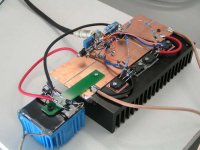
I attached a picture of one mono block prototype. I used a 25VA transformer for quick testing, limiting output power to approx. 11 watts rms.. Not a "breadboard" this time, but a blank PCB mounted directly to the heatsink.
The picture also shows how simple this design is, I built this prototype in half an hour.
There is still a little grain
You might check your power amplifier,
I just completed a fully DC-coupled, all-FET, zero global feedback, balanced bridge power amplifier. It has a dual JFET in the differential input stage and one dual JFET in the balanced driver stage. The driver stage directly drives the H bridge (4 x power MOSFET). I didn't use constant current sources nor current mirrors.
The design uses local feedback to set the total gain. The design offers very high PSRR, and runs from a single 40V DC power supply.
It has balanced inputs, but can also be driven single-ended. In this case the inverting input must be connected to GND in order to avoid picking-up interference.
Stability is so high that I could leave-out both input filter and the Zobel networks on the outputs. The back-emf of the speaker is rectified and fed back to the amplifier power supply.
Both halves of the H-bridge run at approx. 100mA bias current, set by diodes (1.2V voltage drop).
Due to the bridge configuration it's easy to achieve high enough gain to drive the amp to clipping levels with only 500mV input signal. This way lower DAC output voltages can be used.
The DC-offset at the speaker equals around. 80mV without offset trimming. When tuning the input stage and / or driver stage source resistors, DC-offset can be further reduced. DC Drift is very low.
This power amplifier provides exceptional resolution and clarity. There is no audible grain or glare. The full DC-coupling also avoids sound coloration introduced by coupling caps.
I attached a picture of one mono block prototype. I used a 25VA transformer for quick testing, limiting output power to approx. 11 watts rms.. Not a "breadboard" this time, but a blank PCB mounted directly to the heatsink.
The picture also shows how simple this design is, I built this prototype in half an hour.
Attachments
-ecdesigns- said:Hi maxlorenz,
You might check your power amplifier,
I just completed a fully DC-coupled, all-FET, zero global feedback, balanced bridge power amplifier. It has a dual JFET in the differential input stage and one dual JFET in the balanced driver stage. The driver stage directly drives the H bridge (4 x power MOSFET). I didn't use constant current sources nor current mirrors.
The design uses local feedback to set the total gain. The design offers very high PSRR, and runs from a single 40V DC power supply.
It has balanced inputs, but can also be driven single-ended. In this case the inverting input must be connected to GND in order to avoid picking-up interference.
Stability is so high that I could leave-out both input filter and the Zobel networks on the outputs. The back-emf of the speaker is rectified and fed back to the amplifier power supply.
Both halves of the H-bridge run at approx. 100mA bias current, set by diodes (1.2V voltage drop).
Due to the bridge configuration it's easy to achieve high enough gain to drive the amp to clipping levels with only 500mV input signal. This way lower DAC output voltages can be used.
The DC-offset at the speaker equals around. 80mV without offset trimming. When tuning the input stage and / or driver stage source resistors, DC-offset can be further reduced. DC Drift is very low.
This power amplifier provides exceptional resolution and clarity. There is no audible grain or glare. The full DC-coupling also avoids sound coloration introduced by coupling caps.
I attached a picture of one mono block prototype. I used a 25VA transformer for quick testing, limiting output power to approx. 11 watts rms.. Not a "breadboard" this time, but a blank PCB mounted directly to the heatsink.
The picture also shows how simple this design is, I built this prototype in half an hour.
Hi John,
this near to my dreams. Simple and pure.
It seems still simple clever designs sounds better than more regulated, CSs... It brings more problems that able to solved generaly.
Although i dont have any complain to my power amps MPA80.
Maybe could be good to build double DAC balanced version. One DAC for 1 channel and other for 2 channel and goes direct to power amp.
Best wishes,
Bostjan
Re: to get 2V RMS output from 1543
Hi, a bit late to quote this, but I cannot see that you get any reply to your question. Do you get this resolved?
I recently come to know this thread and found this battery solution very interesting. I am not sure if I understand all but I try to describe here how I see this is calculated:
The battery is a current source but not sink, so the flow of current is directionally always from the battery voltage thru the load resistor. So we should set the battery voltage as the MAX DC voltage at the analog out of TDA1543 to fit the swing you want. Looking at the spec sheet, the MIN DC voltage is 1.8V, so if you need 2Vrms output (=5.65Vpp), the MAX DC level will be 7.45V. But the MAX DC level cannot exceed Vdd-1.2V, or 6.8V if you use 8V. Hence I believe the max swing you can get is 5Vpp. The closest battery voltage you can get will be 4x1.5V=6V, so essentially your max swing will be 4.2Vpp or 1.48Vrms (I think this should be enough).
With this, your load resistor will be 4.2V/2.3mA=1826R where 1.8K might be the closest stock value (ie you should not stick to 2.7k load resistor).
But I cannot understand why with a 680R load resistor is possible with 3V battery level. With 680R, the voltage swing will be 680x23mA=1.56Vpp. This will drive the lowest DC level down to 1.5V, which is not possible per spec sheet (1.8V). This point I cannot understand.
Maybe I am totally wrong in how to calculate this. Would appreciate some input.
2A3SET said:with 8V supply and 2.7K load on 1543 (Peter Daniel's DAC), my understanding is we need 8.4V battery, am I correct?
to get 5V peak-peak (8-1.2-1.8), middle point is 1.8+5/2=4.3V, with 0.015MA over 2.7K, the battery is 4.3V + 0.0015*2700 = 8.35
Hi, a bit late to quote this, but I cannot see that you get any reply to your question. Do you get this resolved?
I recently come to know this thread and found this battery solution very interesting. I am not sure if I understand all but I try to describe here how I see this is calculated:
The battery is a current source but not sink, so the flow of current is directionally always from the battery voltage thru the load resistor. So we should set the battery voltage as the MAX DC voltage at the analog out of TDA1543 to fit the swing you want. Looking at the spec sheet, the MIN DC voltage is 1.8V, so if you need 2Vrms output (=5.65Vpp), the MAX DC level will be 7.45V. But the MAX DC level cannot exceed Vdd-1.2V, or 6.8V if you use 8V. Hence I believe the max swing you can get is 5Vpp. The closest battery voltage you can get will be 4x1.5V=6V, so essentially your max swing will be 4.2Vpp or 1.48Vrms (I think this should be enough).
With this, your load resistor will be 4.2V/2.3mA=1826R where 1.8K might be the closest stock value (ie you should not stick to 2.7k load resistor).
But I cannot understand why with a 680R load resistor is possible with 3V battery level. With 680R, the voltage swing will be 680x23mA=1.56Vpp. This will drive the lowest DC level down to 1.5V, which is not possible per spec sheet (1.8V). This point I cannot understand.
Maybe I am totally wrong in how to calculate this. Would appreciate some input.
-ecdesigns- said:
The picture also shows how simple this design is, I built this prototype in half an hour.
Hi John, I see no filter caps after the Transformer / Rectifier ?
Hi FYC,
Without signal, only half of the 2.3mA full-scale current flows through 680 Ohm: 0.00115 * 680 = 0.782V. When adding 0.782 to approx. 1.8 ... 2V DC on the DAC output we get 2.582 ... 2.782V DC, still below 3 ... 3.2V battery reference voltage.
The ac output signal (+/-0.78V) swings around 1.8 ... 2V DC voltage at the DAC output, this gives plenty of headroom.
But I cannot understand why with a 680R load resistor is possible with 3V battery level. With 680R, the voltage swing will be 680x23mA=1.56Vpp. This will drive the lowest DC level down to 1.5V, which is not possible per spec sheet (1.8V). This point I cannot understand.
Without signal, only half of the 2.3mA full-scale current flows through 680 Ohm: 0.00115 * 680 = 0.782V. When adding 0.782 to approx. 1.8 ... 2V DC on the DAC output we get 2.582 ... 2.782V DC, still below 3 ... 3.2V battery reference voltage.
The ac output signal (+/-0.78V) swings around 1.8 ... 2V DC voltage at the DAC output, this gives plenty of headroom.
Hi dddac,
There are 2 x 10,000uF caps soldered below the PCB (not visible on the photograph). The center tap is only used to reference the balanced inputs. The amplifier runs on a single 40V power supply.
The amplifier is designed to reject all (common) power supply noise and hum (fully balanced design + H-bridge output stage). It performs very well on lousy power supplies, as all (switching) noise and hum is common, so it will be rejected by the circuit.
Hi John, I see no filter caps after the Transformer / Rectifier ?
There are 2 x 10,000uF caps soldered below the PCB (not visible on the photograph). The center tap is only used to reference the balanced inputs. The amplifier runs on a single 40V power supply.
The amplifier is designed to reject all (common) power supply noise and hum (fully balanced design + H-bridge output stage). It performs very well on lousy power supplies, as all (switching) noise and hum is common, so it will be rejected by the circuit.
-ecdesigns- said:Hi FYC,
Without signal, only half of the 2.3mA full-scale current flows through 680 Ohm: 0.00115 * 680 = 0.782V. When adding 0.782 to approx. 1.8 ... 2V DC on the DAC output we get 2.582 ... 2.782V DC, still below 3 ... 3.2V battery reference voltage.
The ac output signal (+/-0.78V) swings around 1.8 ... 2V DC voltage at the DAC output, this gives plenty of headroom.
Hi EC, thanks, but still I cannot understand.
At idle (no signal), 1.15mA flows so voltage drop across 680R is 0.78V. Hence the bias voltage at DAC analog out at idle will be 3-0.78=2.22V if a 3V battery set is used. Yes with signal the voltage will swing, but around 2.22V? --and at max current full swing, this will push the DAC analog level to 2.22-0.78V=1.44V. The point is --> Can the DAC DC level run below 1.8V?
Please help with more explainations.
FYC said:
Can the DAC DC level run below 1.8V?
Please help with more explainations.
My experience, is that teh datsheet specs are not in line with the real world where it comes to distortion of the output due to clipping (or close to...)
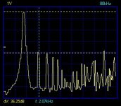
John, why not run a 1kHz 0dB signal and show the FFT result?
That is what I did as well to find optimum load for the TDA1543, just find best compromize between output voltage and THD.....
Attachments
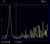
and here to compare a lower output voltage configuration with consequently lower THD
of course this is only valid for the setup I used (VB = 8Volt and mid bias 3,85Volt)
Johns bias setup is different. This is just to show it is not a digital world we live in
of course this is only valid for the setup I used (VB = 8Volt and mid bias 3,85Volt)
Johns bias setup is different. This is just to show it is not a digital world we live in
Attachments
dddac said:
John, why not run a 1kHz 0dB signal and show the FFT result?
John, why not run a 1kHz -60 dB signal and show the FFT result?
dddac said:
That is what I did as well to find optimum load for the TDA1543, just find best compromize between output voltage and THD.....
What does the dV -36.25 mean ?
K2 is -36.25 dB below the fundamental ?
Hi FYC
Sorry, I was too hasty and made a mistake. The bias voltage across the I/V resistor is added to the 1.8V bias voltage of the TDA1543:
1.8 + (0.00115 * 680) = 2.582V.
So the ac signal swings around 2.582V:
2.582 - 0.782 = 1.8V, and 2.582 + 0.782 = 3.364V.
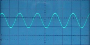
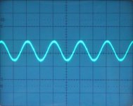
I added an oscillogram of the SD-player output, lower division equals 0V, upper division equals 5V, setting equals 1V/div, the signal swings between 1.8V and 3.5V.
The external bias voltage needs to be 2.582V or slightly higher (margin), I used approx. 3.2V DC.
Based on this, the maximum output voltage with passive I/V conversion, 1.8V DC at the DAC output, and a 9V power supply theoretically equals:
9 - 1.8 = 7.2Vpp or 2.54V rms with a single DAC chip. I/V resistor value: 7.2 / 0.0023 = 3K1.
External bias voltage would need to be approx. (0.00115 * 3100) + 1.8 = 5.365V or slightly higher (margin), 6V DC for example.
Hi EC, thanks, but still I cannot understand.
Sorry, I was too hasty and made a mistake. The bias voltage across the I/V resistor is added to the 1.8V bias voltage of the TDA1543:
1.8 + (0.00115 * 680) = 2.582V.
So the ac signal swings around 2.582V:
2.582 - 0.782 = 1.8V, and 2.582 + 0.782 = 3.364V.
I added an oscillogram of the SD-player output, lower division equals 0V, upper division equals 5V, setting equals 1V/div, the signal swings between 1.8V and 3.5V.
The external bias voltage needs to be 2.582V or slightly higher (margin), I used approx. 3.2V DC.
Based on this, the maximum output voltage with passive I/V conversion, 1.8V DC at the DAC output, and a 9V power supply theoretically equals:
9 - 1.8 = 7.2Vpp or 2.54V rms with a single DAC chip. I/V resistor value: 7.2 / 0.0023 = 3K1.
External bias voltage would need to be approx. (0.00115 * 3100) + 1.8 = 5.365V or slightly higher (margin), 6V DC for example.
Attachments
Hi Bernhard,
I guess I have to buy a suitable spectrum analyzer first. Perhaps somebody could give me some tips about suitable and affordable equipment.
I did attach the 1 KHz -60dB signal from the SD-player (TDA1543, cryo-treated, 680 Ohm I/V resistor, 3.2V external reference voltage, battery powered, unfiltered).
Scope setting, 1mV/div.
This might give some impression about low level performance.
John, why not run a 1kHz -60 dB signal and show the FFT result?
I guess I have to buy a suitable spectrum analyzer first. Perhaps somebody could give me some tips about suitable and affordable equipment.
I did attach the 1 KHz -60dB signal from the SD-player (TDA1543, cryo-treated, 680 Ohm I/V resistor, 3.2V external reference voltage, battery powered, unfiltered).
Scope setting, 1mV/div.
This might give some impression about low level performance.
Attachments
- Home
- Source & Line
- Digital Line Level
- Building the ultimate NOS DAC using TDA1541A