Hi Telstar,
The DI8M was outperformed by the early DI4MJ prototype based on 4 x TDA1543. So it appeared that the DI8M still wasn't getting maximum performance out of the 8 TDA1541A chips. Tweaking the DI8M didn't solve the "problem".
So the DI8M was transformed to a DI4T, using similar techniques as in the DI4MJ early prototype.
Then a rat-race between both DI4MJ and DI4T began, this resulted in the most relevant performance improvements of both DACs.
It ended (for now) in favor of the DI4T. The DI4T is highly accurate and more refined when compared to the DI4MJ. The DI4MJ already provides a level of performance that one would never expect from only 4 x TDA1543 economy version chips. The DI4MJ uses the latest 4-JFET diff-amplifiers, that are basically a replica of the DI4T tube amplifiers, but now using audio JFETs.
Latest DI4T details can be found in this thread, well except for those added last week. There is the optical DEM clock injection circuit. The DEM clock input reference is AGND (DEM clock is part of the analogue DAC circuits), while the DEM clock generator is referenced to DGND (this makes external DEM clock circuits so critical). The optical DEM clock injector circuit solves this problem by providing galvanic insulation between both circuits, while passing the 352.8 KHz DEM clock signal.
The DI4T now has 14 separate power supply filters using gyrators and high-inductance chokes, ringcore chokes, and ferrite beads. The passive filters should attenuate noise that still passes the gyrators and voltage regulators. Multiple coils were placed in series, each coil specifically suited for a certain frequency range.
Every sub-circuit has a separate power supply filter that prevents unwanted current loops and blocks power-supply noise and hum. Special ground schemes were used to minimize interference. Some power supplies have extra Schottky diodes added that prevent backflow of current when the voltage across the power supply buffer capacitor drops. The masterclock receives power through gyrator, voltage regulator, multiple cascaded chokes, and a Schottky diode. It has a local supercap buffer capacitor that's able to power the masterclock for approx. 2 minutes after the power supply has been switched-off. The supercap emulates (and matches) battery power supply performance. The gyrators require approx. 10 seconds to "charge", they provide very low voltage drop due to high-gain darlingtons.
These "measures" lead to exceptional pure and crystal clear sound with the blackest background imaginable.
What happened to the DI8M?
I have been out of the forums for a few months.
The DI8M was outperformed by the early DI4MJ prototype based on 4 x TDA1543. So it appeared that the DI8M still wasn't getting maximum performance out of the 8 TDA1541A chips. Tweaking the DI8M didn't solve the "problem".
So the DI8M was transformed to a DI4T, using similar techniques as in the DI4MJ early prototype.
Then a rat-race between both DI4MJ and DI4T began, this resulted in the most relevant performance improvements of both DACs.
It ended (for now) in favor of the DI4T. The DI4T is highly accurate and more refined when compared to the DI4MJ. The DI4MJ already provides a level of performance that one would never expect from only 4 x TDA1543 economy version chips. The DI4MJ uses the latest 4-JFET diff-amplifiers, that are basically a replica of the DI4T tube amplifiers, but now using audio JFETs.
Latest DI4T details can be found in this thread, well except for those added last week. There is the optical DEM clock injection circuit. The DEM clock input reference is AGND (DEM clock is part of the analogue DAC circuits), while the DEM clock generator is referenced to DGND (this makes external DEM clock circuits so critical). The optical DEM clock injector circuit solves this problem by providing galvanic insulation between both circuits, while passing the 352.8 KHz DEM clock signal.
The DI4T now has 14 separate power supply filters using gyrators and high-inductance chokes, ringcore chokes, and ferrite beads. The passive filters should attenuate noise that still passes the gyrators and voltage regulators. Multiple coils were placed in series, each coil specifically suited for a certain frequency range.
Every sub-circuit has a separate power supply filter that prevents unwanted current loops and blocks power-supply noise and hum. Special ground schemes were used to minimize interference. Some power supplies have extra Schottky diodes added that prevent backflow of current when the voltage across the power supply buffer capacitor drops. The masterclock receives power through gyrator, voltage regulator, multiple cascaded chokes, and a Schottky diode. It has a local supercap buffer capacitor that's able to power the masterclock for approx. 2 minutes after the power supply has been switched-off. The supercap emulates (and matches) battery power supply performance. The gyrators require approx. 10 seconds to "charge", they provide very low voltage drop due to high-gain darlingtons.
These "measures" lead to exceptional pure and crystal clear sound with the blackest background imaginable.
Well, I am tweaking my DIDACs from DI16 and DI8x4 to DI4 or DI4x4... 
On one of my DACs I added TeddyRegs for the output section (still LM4562, active IV) and the TeddyReg for the DAC chips was reduced to 5V (4,8 under load...).
Next (I hope this week) I will try the DATA and WS attenuators. I got 220R SMD resistors for BCK...is it still OK, John?
I never asked this before, what is the reason to make the attenuator referred both to ground and to VCC? Has to be that the signal can be High or Low, right?
Is it OK if I put 22R in series to all signal from the timing chain???
I will show some picks of my test DI4.
Well, I am tweaking my DIDACs from DI16 and DI8x4 to DI4 or DI4x4...
On one of my DACs I added TeddyRegs for the output section (still LM4562, active IV) and the TeddyReg for the DAC chips was reduced to 5V (4,8 under load...).
Next (I hope this week) I will try the DATA and WS attenuators.
Apart, I got 220R SMD resistors for BCK...is it still OK, John?
I never asked this before, what is the reason to make the attenuator referred both to ground and to VCC? Has to be that the signal can be High or Low, right?
Is it OK if I put 22R in series to all signals from the timing chain???
I will show some picks of my test DI4.
http://picasaweb.google.com/maxlorenz24/DIDAC#5259442732563380642
You can see the 4 Teddyregs...two for the DACs and two for the opamps. TeddyRegs rule!
http://picasaweb.google.com/maxlorenz24/DIDAC#5259444020562984882
This one shows the mess with the PCB to adapt it...and DACs PS bypass caps arrangement. I increased 4K7 Rref to 18K...I still do not get the do-not-connect-it thing...
Advices are welcome...
Cheers,
M
Edit>
Sorry, double post while uploading images. Could the kind administrator delete the previous one?
Hi maxlorenz,
I stopped using OP-amps for high performance audio applications, the required negative feedback loop, and the many "issues" with the OP-amp On-chip circuit make them less suitable for these applications. My first choice is tube amplification, my second choice is discrete ALL-JFET amplification.
I use gyrators with very high gain (50,000 and higher) darlingtons. The interference that still passes every semiconductor is then attenuated by using suitable chokes.
Yes it's still OK, I use this value in the DI4MJ.
This is required to create an external 1.2V reference voltage. This reference voltage is then modulated +/- 400mV by the WS or DATA signal. It's also possible to use diodes for reference, but this requires more parts, and is less effective in attenuating ground-bounce (diode stray capacitance).
The TDA1543 / TDA1541A digital input circuit schematic can be found in the TDA1543 datasheet page 5 (a).
I use 3K3 on all digital outputs of the 4x interpolator-scrambler.
Modifying PCBs can get messy, I know all about this, you should see some of my PCBs after modding. Unfortunately nice looking PCBs without a single mod often perform worse than a messy looking PCB that were tuned for best performance.
(still LM4562, active IV)
I stopped using OP-amps for high performance audio applications, the required negative feedback loop, and the many "issues" with the OP-amp On-chip circuit make them less suitable for these applications. My first choice is tube amplification, my second choice is discrete ALL-JFET amplification.
On one of my DACs I added TeddyRegs for the output section
I use gyrators with very high gain (50,000 and higher) darlingtons. The interference that still passes every semiconductor is then attenuated by using suitable chokes.
I got 220R SMD resistors for BCK...is it still OK, John?
Yes it's still OK, I use this value in the DI4MJ.
what is the reason to make the attenuator referred both to ground and to VCC?
This is required to create an external 1.2V reference voltage. This reference voltage is then modulated +/- 400mV by the WS or DATA signal. It's also possible to use diodes for reference, but this requires more parts, and is less effective in attenuating ground-bounce (diode stray capacitance).
The TDA1543 / TDA1541A digital input circuit schematic can be found in the TDA1543 datasheet page 5 (a).
Is it OK if I put 22R in series to all signal from the timing chain???
I use 3K3 on all digital outputs of the 4x interpolator-scrambler.
This one shows the mess with the PCB to adapt it...
Modifying PCBs can get messy, I know all about this, you should see some of my PCBs after modding. Unfortunately nice looking PCBs without a single mod often perform worse than a messy looking PCB that were tuned for best performance.
Dear -ECdesigns-
You were right, again. The Attenuator seem to be a good discover.
DI4(suffix?) sounds like music
http://picasaweb.google.com/maxlorenz24/DIDAC#5260669919727099154
I'll comment later...
Cheers,
M
You were right, again. The Attenuator seem to be a good discover.
DI4(suffix?) sounds like music
http://picasaweb.google.com/maxlorenz24/DIDAC#5260669919727099154
I'll comment later...
Cheers,
M
Dorsai! said:
I know, that slave mode is possible through firewire. Are there any firewire chips available which can possibly be used for DIY?
Yep, have a look here:
http://www.diyaudio.com/forums/showthread.php?postid=1639077#post1639077
Suis-je digne de mon maitre?
Take a look at:
http://picasaweb.google.com/maxlorenz24/DIDAC#5262147115240951426
Now I can write about my experience with DIDACs. The following are opinions based on my auditions, with my setups (which is surely not optimized like ecdesigns') and my humble system.
Without considering the source of I2S, pros and cons of the different DIDACs (all are TDA1543 DACs) I've tried are:
DI16:
Immense soundstage (extending passed the sides of the speakers) with ample instrument/singer separation; relaxed and elegant sound. Good "structure" of the music ( common to all DIDACs I've tried). The bads are: not so good HF extension; "slow"; images are diffuse. Maybe all of these are consequence of HF roll-off. I used PRP (or RPR?) red resistors which sound warmish and may have been a bad choice.
DI4 with TeddyRegs:
Better HF extension which renders images clearer and sounds "faster"; better retrieval of textures and timbres of instruments; the sound is cleaner overall. The bads: weaker bass; soundstage is more reasonable (but I was used to the big one).
DI4*4 with TeddyRegs:
Similar to the previous but more energy on HF and Bass; punchier. Bad: sound is not so clean compared to the former.
DI4 with attenuators and TeddyRegs:
Excellent imaging (pin-pointing) with amazing solidity or density of images, textures and harmonic content; cleaner; intimate sound; charming sounding DAC. The bads: could have more punch and bass.
DI4 with attenuators, TeddyRegs and discrete JFET differential amp:
The best to date. The discrete output amp takes it to another league, really. I love these little JFETs. No wonder gurus recommend them. It makes music so much close to reality, with more dynamic flow and much clearer phrases. Punch, bass extension and bass harmonics also improved a lot.
What's next:
1) passive I/V, first with common R and later with Moebius loop type of resistor.
2) I2S scrambler/interpolator.
I'm having great fun and I even think I am actually understanding some of the things I'm doing!
Cheers,
M
DI4T
Hi ECDesigns,
I have been following this thread for a while and am interested in the stacking 4 x TDA1541 DAC, I already have the 4 DAC chips, so this is an easy option for me!
I am planning of building a synchronus reclocker circuit that will deliver the I2s signal directly to the input on the DAC chip, as per the sugestions and work of John Swenson more info can be found here: http://audiogestalt.wordpress.com/
I would like to know if I could use one of your boards to run the 4 TDA1541 chips with the synch reclocker circuit as above. I know that a large part of your DAC project now revolves around the internal reclocker and microprocessor, however I know that you have invested considerable time in stacking the DAC chips for the best performance and it is this part of the project that caught my attention.
Brad
Re: Suis-je digne de mon maitre?
Roll-off is a clearly audible degradation.
I did A/B test.
Should be no surprise but one might hope that a few dB doesn't hurt.
maxlorenz said:
DI16:
Immense soundstage (extending passed the sides of the speakers) with ample instrument/singer separation; relaxed and elegant sound. Good "structure" of the music ( common to all DIDACs I've tried). The bads are: not so good HF extension; "slow"; images are diffuse. Maybe all of these are consequence of HF roll-off. I used PRP (or RPR?) red resistors which sound warmish and may have been a bad choice.
Roll-off is a clearly audible degradation.
I did A/B test.
Should be no surprise but one might hope that a few dB doesn't hurt.
Agreeeee
Good Idea
MGH said:I hope you settle down on a final version so we can all enjoy your DAC.
Good Idea
Hi Maxlorenz,
Yes there is increased HF roll-off because of 16x linear interpolation, this reduces sinewave energy at higher frequencies as the waveform starts taking a triangular wave shape. This is why I reverted to 4 x linear interpolation. Other cause for HF roll-off is the NOS mode, even when using non-oversampling (fs), both fs and the audio spectrum will intermodulate, causing HF roll-off.
The resistors have significant impact on sound quality (probably caused by properties like inductance, noise and stray capacitance) in combination with the high frequencies being processed.
I have tested many different resistor brands (same position, same value, direct comparison with switch), and ended up using Vishay bulk metal foil, Arcol, copper wire resistors and Beyschlag 1W metal film resistors. The choise of the resistor also depends on the position where it is used.
The lower linear interpolation factor increases HF energy (waveform shape at higher frequencies), so there is a better HF extension. The Teddyregs just proove how important clean power supplies are.
Paralleling DACs without scrambler may worsen L/R channel tolerances (correlated errors), there is also more crosstalk and interference (I2S interface), and clock jitter will increase significantly (more inputs to drive with the same buffer). I wouldn't recommend connecting more than 4 DAC BCK inputs to a clock buffer, the fewer loads, the better. This means using at least 4 BCK buffers.
The punch is probably caused by the higher full-scale current.
This illustrates how big the effect of (I2S) interference can be. By attenuating I2S interface switching noise, the DAC signal output currents pick-up less noise and provide a cleaner sound.
The balanced-input JFET amp you are using has no (global) feedback, and it has few semiconductors (4 x JFET) in the signal path, so it can provide high dynamic resolution.
You are still using OP-amp I/V converters that do use negative feedback. If you use passive I/V resistors with the JFET amp (it's already designed to directly amplify signals from passive I/V resistors), both resolution and transparency should further improve.
Finally you would have to tackle timing jitter (it seems there are no measures taken to block source jitter), and make 100% sure your source provides bit-perfect playback.
DI16:
Immense soundstage (extending passed the sides of the speakers) with ample instrument/singer separation; relaxed and elegant sound. Good "structure" of the music ( common to all DIDACs I've tried). The bads are: not so good HF extension; "slow"; images are diffuse. Maybe all of these are consequence of HF roll-off. I used PRP (or RPR?) red resistors which sound warmish and may have been a bad choice.
Yes there is increased HF roll-off because of 16x linear interpolation, this reduces sinewave energy at higher frequencies as the waveform starts taking a triangular wave shape. This is why I reverted to 4 x linear interpolation. Other cause for HF roll-off is the NOS mode, even when using non-oversampling (fs), both fs and the audio spectrum will intermodulate, causing HF roll-off.
The resistors have significant impact on sound quality (probably caused by properties like inductance, noise and stray capacitance) in combination with the high frequencies being processed.
I have tested many different resistor brands (same position, same value, direct comparison with switch), and ended up using Vishay bulk metal foil, Arcol, copper wire resistors and Beyschlag 1W metal film resistors. The choise of the resistor also depends on the position where it is used.
DI4 with TeddyRegs:
Better HF extension which renders images clearer and sounds "faster"; better retrieval of textures and timbres of instruments; the sound is cleaner overall. The bads: weaker bass; soundstage is more reasonable (but I was used to the big one).
The lower linear interpolation factor increases HF energy (waveform shape at higher frequencies), so there is a better HF extension. The Teddyregs just proove how important clean power supplies are.
DI4*4 with TeddyRegs:
Similar to the previous but more energy on HF and Bass; punchier. Bad: sound is not so clean compared to the former.
Paralleling DACs without scrambler may worsen L/R channel tolerances (correlated errors), there is also more crosstalk and interference (I2S interface), and clock jitter will increase significantly (more inputs to drive with the same buffer). I wouldn't recommend connecting more than 4 DAC BCK inputs to a clock buffer, the fewer loads, the better. This means using at least 4 BCK buffers.
The punch is probably caused by the higher full-scale current.
DI4 with attenuators and TeddyRegs:
Excellent imaging (pin-pointing) with amazing solidity or density of images, textures and harmonic content; cleaner; intimate sound; charming sounding DAC. The bads: could have more punch and bass.
This illustrates how big the effect of (I2S) interference can be. By attenuating I2S interface switching noise, the DAC signal output currents pick-up less noise and provide a cleaner sound.
DI4 with attenuators, TeddyRegs and discrete JFET differential amp:
The best to date. The discrete output amp takes it to another league, really. I love these little JFETs. No wonder gurus recommend them. It makes music so much close to reality, with more dynamic flow and much clearer phrases. Punch, bass extension and bass harmonics also improved a lot.
The balanced-input JFET amp you are using has no (global) feedback, and it has few semiconductors (4 x JFET) in the signal path, so it can provide high dynamic resolution.
You are still using OP-amp I/V converters that do use negative feedback. If you use passive I/V resistors with the JFET amp (it's already designed to directly amplify signals from passive I/V resistors), both resolution and transparency should further improve.
Finally you would have to tackle timing jitter (it seems there are no measures taken to block source jitter), and make 100% sure your source provides bit-perfect playback.
Hi EC,
That is, one Quad buffer per tower, summing the four outs to end with 4*Iout, right?.
What I have not tried yet is if the attenuated WS and DATA signals still drive the 4*DACked towers...
Thanks,
M
I wouldn't recommend connecting more than 4 DAC BCK inputs to a clock buffer, the fewer loads, the better. This means using at least 4 BCK buffers.
That is, one Quad buffer per tower, summing the four outs to end with 4*Iout, right?.
What I have not tried yet is if the attenuated WS and DATA signals still drive the 4*DACked towers...
Thanks,
M
Hi maxlorenz,
The masterclock can only drive limited number of buffers, for 4 x 4 configuration I would suggest using 4 clock buffers, one for each tower. All DAC chips need to have a 220 Ohm damping resistor on the BCK input, this means using 16 damping resistors in total.
If you use the new interpolator / scrambler schematic, you must use non-inverting clock buffers.
If you use fast 74** series shiftregisters, you must use inverting clock buffers, this requires all DAC chips to receive delayed data:
DAC #1, 16 BCK delay
DAC #2, 48 BCK delay
DAC #3, 32 BCK delay
DAC #4, 64 BCK delay
The existing timing module used in both DI8 and DI16 requires a non-inverting BCK clock buffer for DAC #1, and inverting BCK clock buffers for the other DAC chips. This is necessary because DAC #1 doesn't receive a delayed signal, and sampling needs to take place on the positive going edge of BCK. The other chips receive delayed data (changes on the positive going edge of BCK), so they need to sample on the negative going edge of BCK (inverting buffer).
The bad news is that every single DAC chip needs 2 I2S attenuators, that's 32 I2S attenuators in total, or 96 resistors. Both DATA and WS inputs of multiple DAC chips musn't be connected in parallel (unwanted path for interference signal currents).
That is, one Quad buffer per tower, summing the four outs to end with 4*Iout, right?.
The masterclock can only drive limited number of buffers, for 4 x 4 configuration I would suggest using 4 clock buffers, one for each tower. All DAC chips need to have a 220 Ohm damping resistor on the BCK input, this means using 16 damping resistors in total.
If you use the new interpolator / scrambler schematic, you must use non-inverting clock buffers.
If you use fast 74** series shiftregisters, you must use inverting clock buffers, this requires all DAC chips to receive delayed data:
DAC #1, 16 BCK delay
DAC #2, 48 BCK delay
DAC #3, 32 BCK delay
DAC #4, 64 BCK delay
The existing timing module used in both DI8 and DI16 requires a non-inverting BCK clock buffer for DAC #1, and inverting BCK clock buffers for the other DAC chips. This is necessary because DAC #1 doesn't receive a delayed signal, and sampling needs to take place on the positive going edge of BCK. The other chips receive delayed data (changes on the positive going edge of BCK), so they need to sample on the negative going edge of BCK (inverting buffer).
What I have not tried yet is if the attenuated WS and DATA signals still drive the 4*DACked towers...
The bad news is that every single DAC chip needs 2 I2S attenuators, that's 32 I2S attenuators in total, or 96 resistors. Both DATA and WS inputs of multiple DAC chips musn't be connected in parallel (unwanted path for interference signal currents).
Hi MGH,
No, the DI4T is not ready for sale.
Both DI4MJ and DI4T designs are now final.
I still have to manually route the required PCBs while maintaining or improving prototype performance.
EC, is the DI4T ready for sale?
I hope you settle down on a final version so we can all enjoy your DAC.
No, the DI4T is not ready for sale.
Both DI4MJ and DI4T designs are now final.
I still have to manually route the required PCBs while maintaining or improving prototype performance.
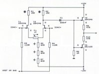
4 JFET amp schematic
Hi Radian,
If you want best performance using passive I/V conversion, the I/V resistor should be connected to a high-impedance load (few mega Ohms).
I attached the 4-JFET amp concept schematic diagram. Similar discrete all JFET amplifiers are used in the new DI4MJ.
The amplifier has balanced inputs and buffered output, it must be connected to clean stabilized power supplies.
I removed the current source as performance significantly dropped (loss of dynamic resolution) when using one.
The coarse gain is set by R1 and R2 : P1. symmetrical clipping is achieved by tuning R5 ... R7 (check with oscilloscope and sine wave test signal). I used multiple resistors in series in order to minimize resistor stray capacitance, this will increase both dynamic resolution and micro detail.
P1 is tuned for minimum ac voltage on the wiper (check with oscilloscope and sine wave test signal), it's recommended to use dual or matched audio JFETS for the input stage.
Both R3 and R4 are the passive I/V resistors. The I/V resistor(s) should be placed as close to the amplifier inputs as possible. The indicated value (110R) is for two TDA1543 outputs in parallel. When using the TDA1543 in this configuration, a clean external 2.5V reference voltage is required.
The amplifier has no global feedback. The output is DC-coupled, depending on DAC and JFET tolerances, DC offset voltages could become too high. The DC output voltage can then be zeroed by applying a small bias voltage to the gates of the output buffer (one resistor to +15V, and one to -15V, each having a slightly different value). Practical example 2.070 M Ohm to +15V, and 2 M Ohm to -15V.
The coupling cap is critical (as usual).
The amplifier is intended to provide approx. 4Vrms max. Other JFETs can be used (2SK 170, 2SJ174), and power supply voltages could be increased to +/-24V (depending on JFET specs).
Hi Radian,
Has there been anything posted on the balanced-input JFET amp?
I would really like to compare it to my passive out solution.
If you want best performance using passive I/V conversion, the I/V resistor should be connected to a high-impedance load (few mega Ohms).
I attached the 4-JFET amp concept schematic diagram. Similar discrete all JFET amplifiers are used in the new DI4MJ.
The amplifier has balanced inputs and buffered output, it must be connected to clean stabilized power supplies.
I removed the current source as performance significantly dropped (loss of dynamic resolution) when using one.
The coarse gain is set by R1 and R2 : P1. symmetrical clipping is achieved by tuning R5 ... R7 (check with oscilloscope and sine wave test signal). I used multiple resistors in series in order to minimize resistor stray capacitance, this will increase both dynamic resolution and micro detail.
P1 is tuned for minimum ac voltage on the wiper (check with oscilloscope and sine wave test signal), it's recommended to use dual or matched audio JFETS for the input stage.
Both R3 and R4 are the passive I/V resistors. The I/V resistor(s) should be placed as close to the amplifier inputs as possible. The indicated value (110R) is for two TDA1543 outputs in parallel. When using the TDA1543 in this configuration, a clean external 2.5V reference voltage is required.
The amplifier has no global feedback. The output is DC-coupled, depending on DAC and JFET tolerances, DC offset voltages could become too high. The DC output voltage can then be zeroed by applying a small bias voltage to the gates of the output buffer (one resistor to +15V, and one to -15V, each having a slightly different value). Practical example 2.070 M Ohm to +15V, and 2 M Ohm to -15V.
The coupling cap is critical (as usual).
The amplifier is intended to provide approx. 4Vrms max. Other JFETs can be used (2SK 170, 2SJ174), and power supply voltages could be increased to +/-24V (depending on JFET specs).
Attachments
Hi Builder Brad,
Before using (synchronous) reclockers, have a look how many logic gates are used in a single D flip-flop (check some datasheets). Each gate adds jitter, and these gates weren't designed to act as low-jitter clock buffers.
I no longer use reclockers, the DAC chips now receive their BCK timing signal straight from suitable clock buffers that are connected to the masterclock. The distance between both masterclock and DAC chips should be kept as short as possible.
The 74**74 isn't the best choice for a reclocker, I performed some jitter tests with various D-flip flop chips. The 74**74 performed worst.
I don't stack DAC chips. I use separate DAC chips that only share the analogue current outputs, DGND and AGND.
You have to use 4 separate TDA1541A circuits, the active divider decoupling caps must not be shared between multiple chips, same applies for the DEM clock connections.
It's best to synchronize the DEM clocks of all 4 DAC chips, I now use a high-speed opto-coupler circuit for injecting the DEM clock in all 4 DAC chips.
The problem with an external DEM clock is that the DEM clock is referenced to AGND (The Dynamic Element Matching circuit is part of the analogue circuit). The DEM clock generator (divider) is referenced to DGND. The opto-coupler now provides the required galvanic insulation between both GNDs, preventing inter modulation between both analogue and digital signal currents.
I achieved best performance when separating both analogue and digital grounds (10mH ring core choke) for HF signals. The choke should have lowest possible DC resistance.
When using the standard DEM clock circuit, multiple DEM clocks with very high jitter amplitude are created, all 4 DEM clock oscillators will also start inter modulating, causing significant sound smearing.
It's best to use separate power supplies for all 4 DAC chips (sharing one single supply causes unwanted crosstalk).
It's very important to use I2S attenuators on all DATA and WS inputs, especially when using multiple chips.
BCK damping resistor value is approx. 22 Ohms (use a separate damping resistor for each TDA1541A BCK input).
I would like to know if I could use one of your boards to run the 4 TDA1541 chips with the synch reclocker circuit as above. I know that a large part of your DAC project now revolves around the internal reclocker and microprocessor, however I know that you have invested considerable time in stacking the DAC chips for the best performance and it is this part of the project that caught my attention.
Before using (synchronous) reclockers, have a look how many logic gates are used in a single D flip-flop (check some datasheets). Each gate adds jitter, and these gates weren't designed to act as low-jitter clock buffers.
I no longer use reclockers, the DAC chips now receive their BCK timing signal straight from suitable clock buffers that are connected to the masterclock. The distance between both masterclock and DAC chips should be kept as short as possible.
The 74**74 isn't the best choice for a reclocker, I performed some jitter tests with various D-flip flop chips. The 74**74 performed worst.
I don't stack DAC chips. I use separate DAC chips that only share the analogue current outputs, DGND and AGND.
You have to use 4 separate TDA1541A circuits, the active divider decoupling caps must not be shared between multiple chips, same applies for the DEM clock connections.
It's best to synchronize the DEM clocks of all 4 DAC chips, I now use a high-speed opto-coupler circuit for injecting the DEM clock in all 4 DAC chips.
The problem with an external DEM clock is that the DEM clock is referenced to AGND (The Dynamic Element Matching circuit is part of the analogue circuit). The DEM clock generator (divider) is referenced to DGND. The opto-coupler now provides the required galvanic insulation between both GNDs, preventing inter modulation between both analogue and digital signal currents.
I achieved best performance when separating both analogue and digital grounds (10mH ring core choke) for HF signals. The choke should have lowest possible DC resistance.
When using the standard DEM clock circuit, multiple DEM clocks with very high jitter amplitude are created, all 4 DEM clock oscillators will also start inter modulating, causing significant sound smearing.
It's best to use separate power supplies for all 4 DAC chips (sharing one single supply causes unwanted crosstalk).
It's very important to use I2S attenuators on all DATA and WS inputs, especially when using multiple chips.
BCK damping resistor value is approx. 22 Ohms (use a separate damping resistor for each TDA1541A BCK input).
- Home
- Source & Line
- Digital Line Level
- Building the ultimate NOS DAC using TDA1541A