Hi maxlorenz,
Only put DAC chips in sockets U17, U21, U25 and U29. ( upper row).
You will have two groups now: group 1 (U17 & U21, non-inverted outputs) and group 2 (U25 & U29, inverted outputs).
There are basically two reasons for using multiple DACs in parallel:
- Reducing bit errors / distortion.
- Generating higher full-scale currents, while providing low output impedance for passive I/V applications.
Placing TDA1543 chips in a tower configuration creates other problems that might not result in better performance.
Perhaps it's better to use selected TDA1543 chips:
The TDA1543 chips aren't graded like the TDA1541A. But like the TDA1541A chips there are certain tolerances, so you also have TDA1543 chips that could receive a "double crown" after selecting.
So I suggest to pick-out 4 TDA1543 chips that provide best perceived sound quality, or measure lowest bit errors / THD @ 1KHz if possible.
The TDA1543, like the TDA1541A was manufactured at different locations, so quality also varies depending on manufacturer. I got lowest average THD @ 1 KHz with TDA1543 chips that were manufactured in Taiwan.
To get an impression of THD @ 1 KHz (0dB), I managed to achieve 0.003% using only 4 x TDA1543, twin differential passive I/V, and discrete JFET diff amp included.
You need an attenuator / level shifter for each separate TDA1543 DATA and WS input pin. So when using 4 x TDA1543, you will need 8 of these identical circuits.
Put two resistors in series 3K3 to +5V, 1K to GND. The point where the two resistors are connected is your star point. The I2S DATA / WS signal is connected to this star point through another 3K3 resistor. The star point connects directly to the DAC I2S input pin.
BCK is not attenuated (seems to work best), connect 4 x 22R resistor to BCK, then connect the other side of each resistor to each TDA1543 BCK input.
Yes, when using 4 x TDA1543, it can be used to serve as reference voltage for 4 x 100 ... 110R (differential passive I/V), or 8 x 220R (twin differential I/V). Use a 100 ... 120R resistor to bias the LM336-2.5. Connect all 4 I/V resistors to this reference voltage. Connect the other side of these I/V resistors to the DAC group outputs.
By differential passive I/V conversion I mean placing an I/V resistor on each paralleled group output, creating both an inverted and non-inverted signal for left and right channel. With twin differential I/V, I mean placing a separate I/V resistor on every single DAC chip output, creating multiple inverted and non-inverted signals for left and right channels, the derived multiple voltages are then added in a diff. summing amp.
Example:
Single-ended, 500mV across I/V resistor.
Differential, +500mV and -500mV across I/V resistors, 1V at summing output.
Twin differential I/V, +500mv(1), +500mv(3), -500mV(2), -500mv(4) across I/V resistors, 2V at summing amp output.
The diff.amp will cancel the DC offset voltages, and double or quadruple the output amplitude by adding both inverted and non-inverted signals.
DI8M / DI16:
DACs 2 ... 8 or 2 ... 16 receive delayed DATA / WS through cascaded D-flip-flops. The D-flip-flop data changes on the positive going edge of BCK. The TDA154x chips sample both DATA and WS on the positive going edge of BCK too (when D-flip-flop outputs aren't stable). So the BCK signal for DAC chips 2 ... 8 or 2 ... 16 needs to be inverted, now the DAC chips sample both DATA / WS after the D-flip-flops have stabilized.
Exception is DAC1, as it receives data straight from the I2S bus, so DAC1 (just like a standard NOS DAC) receives a non-inverted BCK signal.
This means that DAC1 is latched first, and DAC2...n are latched 177ns later (@ 2.8224 MHz BCK), so not all DAC chips latch simultaneously.
The DI4T has a new timing-chain with following delays:
DAC1, 16 BCK delay
DAC2, 48 BCK delay, inverted data
DAC3, 32 BCK delay
DAC4, 64 BCK delay, inverted data
All DAC chips now receive their data from D-flip-flops (delayed), including DAC1. Now all DACs receive an inverted BCK signal and all DAC outputs are latched simultaneously.
But instead of 4 chips in a row, isn't it better to put 4 "towers" of 4 (or 8) chips each, two in each row (row means "DAC group", right?). With corresponding I/V R reduction.
Only put DAC chips in sockets U17, U21, U25 and U29. ( upper row).
You will have two groups now: group 1 (U17 & U21, non-inverted outputs) and group 2 (U25 & U29, inverted outputs).
There are basically two reasons for using multiple DACs in parallel:
- Reducing bit errors / distortion.
- Generating higher full-scale currents, while providing low output impedance for passive I/V applications.
Placing TDA1543 chips in a tower configuration creates other problems that might not result in better performance.
Perhaps it's better to use selected TDA1543 chips:
The TDA1543 chips aren't graded like the TDA1541A. But like the TDA1541A chips there are certain tolerances, so you also have TDA1543 chips that could receive a "double crown" after selecting.
So I suggest to pick-out 4 TDA1543 chips that provide best perceived sound quality, or measure lowest bit errors / THD @ 1KHz if possible.
The TDA1543, like the TDA1541A was manufactured at different locations, so quality also varies depending on manufacturer. I got lowest average THD @ 1 KHz with TDA1543 chips that were manufactured in Taiwan.
To get an impression of THD @ 1 KHz (0dB), I managed to achieve 0.003% using only 4 x TDA1543, twin differential passive I/V, and discrete JFET diff amp included.
Could you please post a schematic of the I2S attenuators/level shifters...I read your previous post about this topic but I fail to see how they are connected.
You need an attenuator / level shifter for each separate TDA1543 DATA and WS input pin. So when using 4 x TDA1543, you will need 8 of these identical circuits.
Put two resistors in series 3K3 to +5V, 1K to GND. The point where the two resistors are connected is your star point. The I2S DATA / WS signal is connected to this star point through another 3K3 resistor. The star point connects directly to the DAC I2S input pin.
BCK is not attenuated (seems to work best), connect 4 x 22R resistor to BCK, then connect the other side of each resistor to each TDA1543 BCK input.
Will one LM336 be enough for all 4 I/V R?
Yes, when using 4 x TDA1543, it can be used to serve as reference voltage for 4 x 100 ... 110R (differential passive I/V), or 8 x 220R (twin differential I/V). Use a 100 ... 120R resistor to bias the LM336-2.5. Connect all 4 I/V resistors to this reference voltage. Connect the other side of these I/V resistors to the DAC group outputs.
By differential passive I/V conversion I mean placing an I/V resistor on each paralleled group output, creating both an inverted and non-inverted signal for left and right channel. With twin differential I/V, I mean placing a separate I/V resistor on every single DAC chip output, creating multiple inverted and non-inverted signals for left and right channels, the derived multiple voltages are then added in a diff. summing amp.
Example:
Single-ended, 500mV across I/V resistor.
Differential, +500mV and -500mV across I/V resistors, 1V at summing output.
Twin differential I/V, +500mv(1), +500mv(3), -500mV(2), -500mv(4) across I/V resistors, 2V at summing amp output.
The diff.amp will cancel the DC offset voltages, and double or quadruple the output amplitude by adding both inverted and non-inverted signals.
Also, what does this "simultaneous clocking" mean?
Compared to the previous situation, that is...
DI8M / DI16:
DACs 2 ... 8 or 2 ... 16 receive delayed DATA / WS through cascaded D-flip-flops. The D-flip-flop data changes on the positive going edge of BCK. The TDA154x chips sample both DATA and WS on the positive going edge of BCK too (when D-flip-flop outputs aren't stable). So the BCK signal for DAC chips 2 ... 8 or 2 ... 16 needs to be inverted, now the DAC chips sample both DATA / WS after the D-flip-flops have stabilized.
Exception is DAC1, as it receives data straight from the I2S bus, so DAC1 (just like a standard NOS DAC) receives a non-inverted BCK signal.
This means that DAC1 is latched first, and DAC2...n are latched 177ns later (@ 2.8224 MHz BCK), so not all DAC chips latch simultaneously.
The DI4T has a new timing-chain with following delays:
DAC1, 16 BCK delay
DAC2, 48 BCK delay, inverted data
DAC3, 32 BCK delay
DAC4, 64 BCK delay, inverted data
All DAC chips now receive their data from D-flip-flops (delayed), including DAC1. Now all DACs receive an inverted BCK signal and all DAC outputs are latched simultaneously.
DI4T PCBs
Hi MGH,
I used 8 x TDA1541A with the new design, 4 x interpolation produced a more fluent realistic sound.
No I didn't cut the DI8 mainboard in half. I just left-out 6 modules (4 x DA1541A, and 2 x IVDIF), and performed some PCB modding. So it's possible to build a DI4T using existing PCBs.
This weekend I designed a DI4 mainboard as well, PCB lay-out is basically ready. the PCB measures 5.27" (134 mm) x 6.26" (159 mm).
The DI4 mainboard will contain the following:
- 5V power supplies with LC filters (54mH / 0.1F).
- 4 x DA1541A module.
- Local power supply decoupling capacitor banks for DA1541A modules (48 electr. caps in total).
- Both TOSLINK & SPDIF receiver modules.
- VCXO.
- 4 x clock buffer
- DEM clock generation.
- WS generation.
- MCLK prescaler.
- Phase discriminator.
- Loop filter with integrated LC filter (54mH / 0.022F) for VCXO.
- Timing circuit (4 x interpolation).
- VCXO lock indicator circuit.
The DI4 mainboard only requires -10, -20, and +10V (one 8-way connector)
TOSLINK receiver is integrated on the PCB, no extra connectors
Output for LED indicators (one 4-way connector)
DAC current outputs for L, NL, R and NR (two 3-way connectors).
Now the the following PCBs would be required to build the new DI4T:
1 x DI4MAIN.
4 x DA1541A.
1 x DI8PS.
1 x TUBEPS.
2 x TUBEDIF.
Hi MGH,
Have you tried using 8 DAC chips with your new design? Based on what you have described, going from 4 to 8 DACs may degrade the sound quality? Did you cut the DI8M DAC module PCB in half to build the DI4T? I'm not sure what I need to order to build your latest design.
I used 8 x TDA1541A with the new design, 4 x interpolation produced a more fluent realistic sound.
No I didn't cut the DI8 mainboard in half. I just left-out 6 modules (4 x DA1541A, and 2 x IVDIF), and performed some PCB modding. So it's possible to build a DI4T using existing PCBs.
This weekend I designed a DI4 mainboard as well, PCB lay-out is basically ready. the PCB measures 5.27" (134 mm) x 6.26" (159 mm).
The DI4 mainboard will contain the following:
- 5V power supplies with LC filters (54mH / 0.1F).
- 4 x DA1541A module.
- Local power supply decoupling capacitor banks for DA1541A modules (48 electr. caps in total).
- Both TOSLINK & SPDIF receiver modules.
- VCXO.
- 4 x clock buffer
- DEM clock generation.
- WS generation.
- MCLK prescaler.
- Phase discriminator.
- Loop filter with integrated LC filter (54mH / 0.022F) for VCXO.
- Timing circuit (4 x interpolation).
- VCXO lock indicator circuit.
The DI4 mainboard only requires -10, -20, and +10V (one 8-way connector)
TOSLINK receiver is integrated on the PCB, no extra connectors
Output for LED indicators (one 4-way connector)
DAC current outputs for L, NL, R and NR (two 3-way connectors).
Now the the following PCBs would be required to build the new DI4T:
1 x DI4MAIN.
4 x DA1541A.
1 x DI8PS.
1 x TUBEPS.
2 x TUBEDIF.
Re: DI4T PCBs
Interesting project . I still have 8 tda1541a around . Are there the new project cost information avaiable on your site?
-ecdesigns- said:Hi MGH,
This weekend I designed a DI4 mainboard as well, PCB lay-out is basically ready. the PCB measures 5.27" (134 mm) x 6.26" (159 mm).
The DI4 mainboard will contain the following:
- 5V power supplies with LC filters (54mH / 0.1F).
- 4 x DA1541A module.
- Local power supply decoupling capacitor banks for DA1541A modules (48 electr. caps in total).
- Both TOSLINK & SPDIF receiver modules.
- VCXO.
- 4 x clock buffer
- DEM clock generation.
- WS generation.
- MCLK prescaler.
- Phase discriminator.
- Loop filter with integrated LC filter (54mH / 0.022F) for VCXO.
- Timing circuit (4 x interpolation).
- VCXO lock indicator circuit.
The DI4 mainboard only requires -10, -20, and +10V (one 8-way connector)
TOSLINK receiver is integrated on the PCB, no extra connectors
Output for LED indicators (one 4-way connector)
DAC current outputs for L, NL, R and NR (two 3-way connectors).
Now the the following PCBs would be required to build the new DI4T:
1 x DI4MAIN.
4 x DA1541A.
1 x DI8PS.
1 x TUBEPS.
2 x TUBEDIF.
Interesting project . I still have 8 tda1541a around . Are there the new project cost information avaiable on your site?
Hi folks.
Did anybody look at the Lessloss DAC?
Seems to be a ( or the) leading edge DAC with quite some nice features. Pretty much everything what we're discussing around here.
Interesting is the shunt-to-ground volume control? Did anybody think about over here how to apply it to 1541/43 chips?
Cheers
Did anybody look at the Lessloss DAC?
Seems to be a ( or the) leading edge DAC with quite some nice features. Pretty much everything what we're discussing around here.
Interesting is the shunt-to-ground volume control? Did anybody think about over here how to apply it to 1541/43 chips?
Cheers
I didn't realize that bringing this up would be such a sensitive issue. ")
I do not intend to hijack this thread. I just try to keep one eye open
for other things, which might add value to our discussion around here.
I'd be happy though if anybody could answer my question to the
shunt-to-ground volume control, which was the background for bringing
this DAC up here. And I could (theoretically) agree to the LessLoss guys
position, that this kind of volume-control might be the best solution for I/V
outputs.
Hi -ecdesigns-,
Sorry for the very late reply: Post #1981.
Thanks for your explanations and advices.
I've been busy at work and only had time to improve some of my DIY interconnects. I have to upgrade all my internal hookup wires to Litz type. Perhaps I'd also use it for power supply duties...
OT: I've been listening, through my DI-DAC of course, to an unbelievable musical treasure that I could not resist...
http://www.abeillemusique.com/produit.php?cle=28367
One hundred CDs from legendary Russian artists.
Click the links and you will see the details.
I was astonished by the sound quality of the recordings, considering the recording dates and considering the fact that all CDs come form "live performances"!
Not bad for EU88
(without shipment).
Don't miss Brilliant Classics offers!
Cheers,
M
variable passive I/V resistor volume control
Hi soundcheck,
What about using a variable passive I/V resistor for volume control? Possible options are a stereo stepped variable resistor, or wire wound potentiometers. This way there is no need for an additional (shunt) attenuator. You would also keep full 16 bit resolution with your system.
Hi soundcheck,
Interesting is the shunt-to-ground volume control? Did anybody think about over here how to apply it to 1541/43 chips?
What about using a variable passive I/V resistor for volume control? Possible options are a stereo stepped variable resistor, or wire wound potentiometers. This way there is no need for an additional (shunt) attenuator. You would also keep full 16 bit resolution with your system.
Re: variable passive I/V resistor volume control
Indeed a very viable option. If you use the DAC with DC bias, the variable I/V will not be an option, but using stepped or wirewound volume controll is absolutely an option with as small extra, when playing at lower volumes, which you normally do, that the outputimpedance becomes lower and influence from Couple capacitor in low frequencies gets less
regards
doede
-ecdesigns- said:Hi soundcheck,
What about using a variable passive I/V resistor for volume control? Possible options are a stereo stepped variable resistor, or wire wound potentiometers. This way there is no need for an additional (shunt) attenuator. You would also keep full 16 bit resolution with your system.
Indeed a very viable option. If you use the DAC with DC bias, the variable I/V will not be an option, but using stepped or wirewound volume controll is absolutely an option with as small extra, when playing at lower volumes, which you normally do, that the outputimpedance becomes lower
and influence from Couple capacitor in low frequencies gets lessregards
doede
Hi ec-designs, Hi dddac.
Good to see that you also see the high potential of the I/V stepped volume control.
Now we need to get more specific:
For ten steps I'd need quite some (2*20) low value high quality resistors below 100R to get a reasonable stepping covered.
That's gonna be quite some effort, if values are available.
A wirewound pot most probably falls behind my Econistors in terms of overall performance. I mean - the wirewound pots are highly inductive, aren't they?
Perhaps I start to make my own ( as proposed by John) wirewounds. For ten steps or so this would mean 40 of them.
But perhaps it's possible to take a tap out of the bifilar winding, wich would reduce the amount by half.
Alternative: I just do the big steps 6/12/18db externally and the range in between I do digitally. This way i'd just loose minimum resolution and I'd gain maximum flexibility at lowest effort.
Best case I'd just need 2*3 tapped-diy-wirewounds.
One basic consideration or prequisite is IMO still valid.
One should set the amp gain this high that at 0db DAC out, the maximum
listening volume is achieved. This will improve the stepping range
on the I/V volume control.
Cheers
Hi DDDAC,
If I am correct, this issue can be easily solved by using an external reference voltage. The variable passive I/V resistors would now connect to this external reference voltage instead of GND. This reference voltage can be chosen to provide lowest THD with maximum output amplitude. The TDA1543 Vref pins could now be left unconnected. I already tested this, and it works very well.
Since a part of the ac output current of your DAC also flows through the coupling capacitor and connected load. Lowering I/V resistor value could indeed provide significant improvements.
At moderate volume settings, the ac voltage at the TDA1543 outputs would be reduced quite a bit as well, this in turn lowers THD significantly (output compliance).
Indeed a very viable option. If you use the DAC with DC bias, the variable I/V will not be an option
If I am correct, this issue can be easily solved by using an external reference voltage. The variable passive I/V resistors would now connect to this external reference voltage instead of GND. This reference voltage can be chosen to provide lowest THD with maximum output amplitude. The TDA1543 Vref pins could now be left unconnected. I already tested this, and it works very well.
when playing at lower volumes, which you normally do, that the outputimpedance becomes lower and influence from Couple capacitor in low frequencies gets less
Since a part of the ac output current of your DAC also flows through the coupling capacitor and connected load. Lowering I/V resistor value could indeed provide significant improvements.
At moderate volume settings, the ac voltage at the TDA1543 outputs would be reduced quite a bit as well, this in turn lowers THD significantly (output compliance).
Hi soundcheck,
I was thinking of a binary volume control,
For example: 2.5R, 5R, 10R, 20R, 40R, 80R and so on. This way, many steps can be created using few resistors. Each resistor could have a suitable relay contact across it. The relays could be controlled by a small microcontroller, or by a PC. Logarithmic volume control characteristic could be achieved by skipping intermediate steps.
For ten steps I'd need quite some (2*20) low value high quality resistors below 100R to get a reasonable stepping covered.
I was thinking of a binary volume control,
For example: 2.5R, 5R, 10R, 20R, 40R, 80R and so on. This way, many steps can be created using few resistors. Each resistor could have a suitable relay contact across it. The relays could be controlled by a small microcontroller, or by a PC. Logarithmic volume control characteristic could be achieved by skipping intermediate steps.
New DI4 main board completed
Hi maxlorenz,
I can start listening to all my CD recordings again .... The DI4 main board is ready, and it sounds pretty good, much better than the DI4T prototype setup.
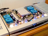
I attached a photograph of my DI8M reference DAC that has been converted into a DI4T. It's running on cryogenic treated tubes as well.
The DI4 main board contains all circuits listed in post #1982, and measures only 5.27" (134 mm) x 6.26" (159 mm).
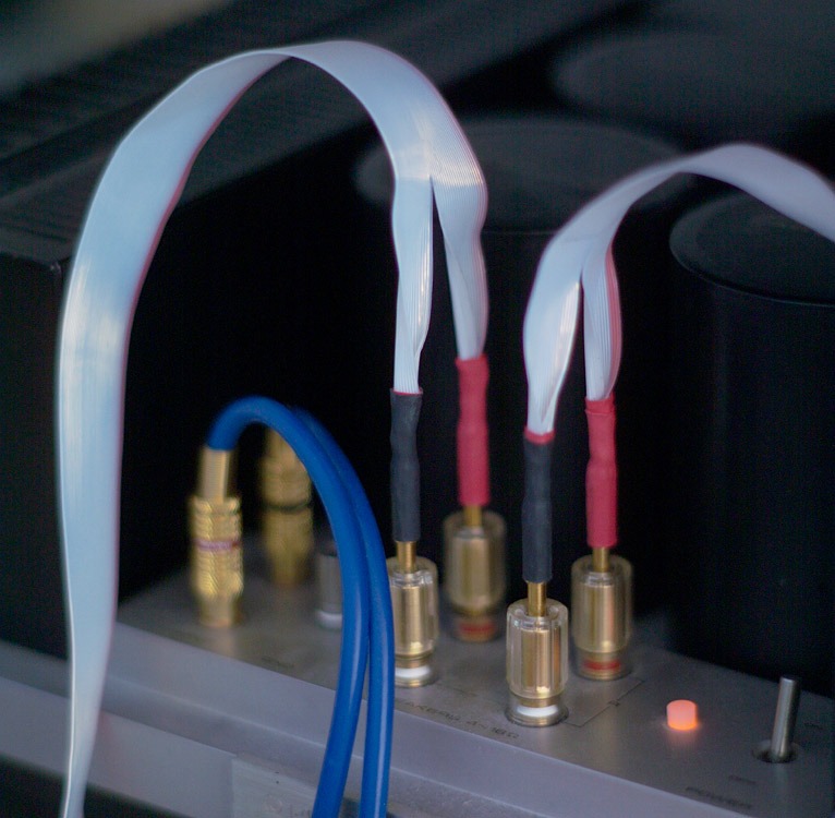
I use TOSLINK exclusively now, the TOSLINK receiver is soldered directly to the DI4 main board. There is a lot more space in the DI8M housing now. The copper wire passive I/V resistors are soldered directly to the input tube socket. The DAC currents are transported through Van Damme OFC studio patch cable.
Clock distribution path on the DI4T module is very short now, 4 UHS clock buffers are used. Both master clock and clock buffers run on a clean power supply (comparable to a battery supply). Passive low-pass filters are used to isolate both VCXO and clock buffers from (power supply) noise.
Interference with other signals is minimized by using wire bridges / resistors that extend approx. 5mm above the PCB surface, and by keeping interference signals as far away from the BCK signal as possible. I even used an attenuator after the TOSLINK receiver to reduce crosstalk.
BCK is a clean square wave with 50% duty cycle, no reclocking is used. The blue LED on the front panel now indicates VCXO lock.
I use Audyn plus coupling caps with silvered mica bypass. The output attenuator is now gone, if my calculations are correct, output impedance of the twin cathode follower (ECC82) is approx. (rp/(mu+1))/2 = (7700/(17+1))/2 = 214 Ohms.
Hi maxlorenz,
OT: I've been listening, through my DI-DAC of course, to an unbelievable musical treasure that I could not resist...
I can start listening to all my CD recordings again .... The DI4 main board is ready, and it sounds pretty good, much better than the DI4T prototype setup.
I attached a photograph of my DI8M reference DAC that has been converted into a DI4T. It's running on cryogenic treated tubes as well.
The DI4 main board contains all circuits listed in post #1982, and measures only 5.27" (134 mm) x 6.26" (159 mm).
I use TOSLINK exclusively now, the TOSLINK receiver is soldered directly to the DI4 main board. There is a lot more space in the DI8M housing now. The copper wire passive I/V resistors are soldered directly to the input tube socket. The DAC currents are transported through Van Damme OFC studio patch cable.
Clock distribution path on the DI4T module is very short now, 4 UHS clock buffers are used. Both master clock and clock buffers run on a clean power supply (comparable to a battery supply). Passive low-pass filters are used to isolate both VCXO and clock buffers from (power supply) noise.
Interference with other signals is minimized by using wire bridges / resistors that extend approx. 5mm above the PCB surface, and by keeping interference signals as far away from the BCK signal as possible. I even used an attenuator after the TOSLINK receiver to reduce crosstalk.
BCK is a clean square wave with 50% duty cycle, no reclocking is used. The blue LED on the front panel now indicates VCXO lock.
I use Audyn plus coupling caps with silvered mica bypass. The output attenuator is now gone, if my calculations are correct, output impedance of the twin cathode follower (ECC82) is approx. (rp/(mu+1))/2 = (7700/(17+1))/2 = 214 Ohms.
Attachments
Excellent man!
Now, find the time to jump to one of the European DIY meetings and show them what is all about 
About cables, it is a shame that I ran out of 26AWG OCC copper (mono crystal) wire...the last interconnect that I made (4 strands for each polarity; manually braided) smashed my previous Silver Sonic Pro Studio cable (silver over OFC; US$ 9/foot) in every aspect of the music.
I mention it because I feel amazed that wire is so important and that there are people that do not hear differences.
I bet your DIY I/V resistor would sound stellar with OCC copper.
If I only could get more of it...
edit: I think I found it, far east!
Now, find the time to jump to one of the European DIY meetings and show them what is all about
About cables, it is a shame that I ran out of 26AWG OCC copper (mono crystal) wire...the last interconnect that I made (4 strands for each polarity; manually braided) smashed my previous Silver Sonic Pro Studio cable (silver over OFC; US$ 9/foot) in every aspect of the music.
I mention it because I feel amazed that wire is so important and that there are people that do not hear differences.
I bet your DIY I/V resistor would sound stellar with OCC copper.
If I only could get more of it...
edit: I think I found it, far east!
maxlorenz said:I feel amazed that wire is so important
Me too.
Don't look at the cinch...
Speaker cable is a ribbon with 42 x solid silverplated wire in teflon.
maxlorenz said:I bet your DIY I/V resistor would sound stellar with OCC copper.
Manganin ?
Interlinks & passive I/V resistors
Hi Bernhard,
The use of silver-plated copper wire only makes sense for HF applications where the skin effect occurs. When used for demanding (LF) audio applications, pure silver wire should be used.
Speaker interlinks have to pass both large (peak) ac currents, and low level currents at the same time. It's important to prevent large (peak) ac currents to mask the low level currents. Noise increases with increased (ac) current, this basically means that resolution is reduced (masking of low level ac currents) as current increases.
On the other hand, the (active) volume control masks resolution at low volume settings. So basically it's quite difficult to achieve high resolution at all.
One effective way to reduce the masking of low level currents, is splitting-up the high (peak) current in multiple smaller currents, using multiple insulated wires. Both current and noise in each wire will now be significantly reduced, so low level details can surface.
Other problem is the (alternating) magnetic field that is generated around each separate wire. If problems occur here, resolution might still be reduced as a result of local electromagnetic field fluctuations between the multiple wires. It seems best to have one (alternating) magnetic field among all wires. This can be achieved with litz wire (wires twisted together).
So I use litz wire for interlinks exclusively, not because of the better HF properties, or lower DC resistance, but because of the ability of these interlinks to preserve low level detail.
Passive I/V resistors have to process very low level signals. For example, if ac full-scale voltage across a passive I/V resistor equals 320mV. This would mean that @ 16 bits, a LSB change would result in 4.8uV voltage change. These low voltages require extreme low noise resistors in order to resolve full resolution at the source.
Better electrical conductance means less friction (heat), and lower noise. So it would be logical to use materials that have best electrical conductivity, when constructing a low noise passive I/V resistor.
Electrical conductivity (@ 20 Celcius with copper as reference = 100), higher value = better:
Silver 106
Copper (annealed) 100
Copper (hard-drawn) 89.5
Gold 65
Chromium 55
Brass 28
Iron (pure) 17.7
Tin 13
Nickel 12 .. 16
Lead 7
Manganin 3.7
Constantin 3.24
NiCr 1.45
This means manganin (3.7) is a pretty poor electrical conductor, compared to copper (100), or silver (106).
So my favorite passive I/V resistor would be made from pure silver litz wire.
Hi Bernhard,
Speaker cable is a ribbon with 42 x solid silverplated wire in teflon.
The use of silver-plated copper wire only makes sense for HF applications where the skin effect occurs. When used for demanding (LF) audio applications, pure silver wire should be used.
Speaker interlinks have to pass both large (peak) ac currents, and low level currents at the same time. It's important to prevent large (peak) ac currents to mask the low level currents. Noise increases with increased (ac) current, this basically means that resolution is reduced (masking of low level ac currents) as current increases.
On the other hand, the (active) volume control masks resolution at low volume settings. So basically it's quite difficult to achieve high resolution at all.
One effective way to reduce the masking of low level currents, is splitting-up the high (peak) current in multiple smaller currents, using multiple insulated wires. Both current and noise in each wire will now be significantly reduced, so low level details can surface.
Other problem is the (alternating) magnetic field that is generated around each separate wire. If problems occur here, resolution might still be reduced as a result of local electromagnetic field fluctuations between the multiple wires. It seems best to have one (alternating) magnetic field among all wires. This can be achieved with litz wire (wires twisted together).
So I use litz wire for interlinks exclusively, not because of the better HF properties, or lower DC resistance, but because of the ability of these interlinks to preserve low level detail.
Manganin ?
Passive I/V resistors have to process very low level signals. For example, if ac full-scale voltage across a passive I/V resistor equals 320mV. This would mean that @ 16 bits, a LSB change would result in 4.8uV voltage change. These low voltages require extreme low noise resistors in order to resolve full resolution at the source.
Better electrical conductance means less friction (heat), and lower noise. So it would be logical to use materials that have best electrical conductivity, when constructing a low noise passive I/V resistor.
Electrical conductivity (@ 20 Celcius with copper as reference = 100), higher value = better:
Silver 106
Copper (annealed) 100
Copper (hard-drawn) 89.5
Gold 65
Chromium 55
Brass 28
Iron (pure) 17.7
Tin 13
Nickel 12 .. 16
Lead 7
Manganin 3.7
Constantin 3.24
NiCr 1.45
This means manganin (3.7) is a pretty poor electrical conductor, compared to copper (100), or silver (106).
So my favorite passive I/V resistor would be made from pure silver litz wire.
Re: Interlinks & passive I/V resistors
However the current density is highest on the surface of the conductor, thats where the silver is.
My own theory about silver plated wire is that the current follows the path of lowest impedance and that is the surface of a silverplated wire also for low frequencies.
Twisted wire is more capacitive.
It seems there is no pure silver ribbon cable available, even the silverplated is hard to get.
I clearly preferred the Manganin over Vishay bulk metal foils.
-ecdesigns- said:
The use of silver-plated copper wire only makes sense for HF applications where the skin effect occurs. When used for demanding (LF) audio applications, pure silver wire should be used.
However the current density is highest on the surface of the conductor, thats where the silver is.
My own theory about silver plated wire is that the current follows the path of lowest impedance and that is the surface of a silverplated wire also for low frequencies.
Twisted wire is more capacitive.
It seems there is no pure silver ribbon cable available, even the silverplated is hard to get.
I clearly preferred the Manganin over Vishay bulk metal foils.
Wires for resistance
resistors by definition have to have resistance which is the electrical equivalent of friction.
friction will intrinsically create heat but it does not intrinsically create noise
silicon oil & sandpaper both have friction but only the oil has smooth, quiet friction.
so the question is not what resistive element has less resistance, it is what resistance has low noise or a smooth action
In my experience constantan wire has truly excellent qualities with regard to how in "sounds" and as a bonus it is manufactured specifically to give a very low temperature co-efficient
No need to worry about using silver wire
mike
- Home
- Source & Line
- Digital Line Level
- Building the ultimate NOS DAC using TDA1541A