Hi Niamex
I have no intention to market a DAC. if you have any question about the design, I will try to answer as much as I can.
Cheers
Hi QUANTRAN,
Sorry for my late response but I feel unease to just exploit your ideas and long time experience. Otherwise the best and cheapest solution for me would be to ask for the schematic which is not fair enough. Anyway I dream for a DAC based on pcm63 with direct I/V conversion buffered by double triode /BENDIX 6385/.
Best regards,
Ignat
Dear Quantran ,
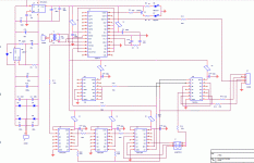
I just found your solution for PCM63 and I 'm very interest to follow. Could you please reccommend me as your lastet schematic why you connect pin12 (sck) of cs8414 to pin9(2Q) of 74HC74.
Thank you
Sorry, my hard drive that contained this design died many years ago. I remember that I was using cs8414 in a special mode where sck should be fed by external clock signal. 74hc74 is just for dividing the clock.
Dear Quantran,Sorry, my hard drive that contained this design died many years ago. I remember that I was using cs8414 in a special mode where sck should be fed by external clock signal. 74hc74 is just for dividing the clock.
Thank you very much ,for your advise .I have read cs8414 datasheet and compare your schematic that you post as attached.May I ask you more.Can I run CS8414 with I2S mode and use FS out from pin6 of the 3rd 74HC164 by use SCK output from CS8414 for PCM63?
Attachments
Dear Quantran,
Thank you very much ,for your advise .I have read cs8414 datasheet and compare your schematic that you post as attached.May I ask you more.Can I run CS8414 with I2S mode and use FS out from pin6 of the 3rd 74HC164 by use SCK output from CS8414 for PCM63?
I think you can with some modifications. In I2S mode, timing of sck and data relative to fsync is different from the mode that I use. The modifications may involve shifting fsync by one more sck cycle and you need to check whethe sck rising edge is the same or not. In some mode data bit is output on rising edge of sck while in other mode data output at falling edge.
Dear Quantran,I think you can with some modifications. In I2S mode, timing of sck and data relative to fsync is different from the mode that I use. The modifications may involve shifting fsync by one more sck cycle and you need to check whethe sck rising edge is the same or not. In some mode data bit is output on rising edge of sck while in other mode data output at falling edge.
Thank you very much for your advise . I already do as your schematic but connect fsync output from pin11 (Q5) of the 3rd 74HC164 and the circuit is work.
Dear Quantran,
Thank you very much for your advise . I already do as your schematic but connect fsync output from pin11 (Q5) of the 3rd 74HC164 and the circuit is work.
Excellent. Pin 11 is right because data line in i2s standard is delayed 1 sck after fsync.
If your sck has low jitter then the result will be very good because sck controls the timing of latch enable signal.
Dear Quantran,I have also found the gerber files for the pcb. If anyone is interested I will share them for personal use only. Please note that I am not a professional pcb engineer so pls set low expextation for layout and routing.
I'm so interest.Could you please send to me at nui9dogs@yahoo.com.?
Dear Quantran,
I'm so interest.Could you please send to me at nui9dogs@yahoo.com.?
I have sent you. Enjoy diy.
Dear Quantran,I have also found the gerber files for the pcb. If anyone is interested I will share them for personal use only. Please note that I am not a professional pcb engineer so pls set low expextation for layout and routing.
I'm so interest too.Could you please send to me at focom@mail.ru.?
8412-pcm63
I'm so interest.Could you please send to me at focom@mail.ru?
Dear Quantran,I have also found the gerber files for the pcb. If anyone is interested I will share them for personal use only. Please note that I am not a professional pcb engineer so pls set low expextation for layout and routing.
I'm so interest.Could you please send to me at focom@mail.ru?
- Status
- This old topic is closed. If you want to reopen this topic, contact a moderator using the "Report Post" button.
- Home
- Source & Line
- Digital Line Level
- Cs8412 - Pcm63 Non-oversampling