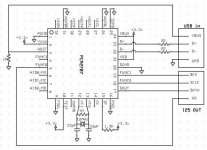
Is this implementation correct if I simply want to use the PCM2707 as I2S interface ? The decoupling caps are obviously missing on the schematic. ")
link to the PCM2707 datasheet : http://focus.ti.com/lit/ds/symlink/pcm2707.pdf
link to the PCM2707 datasheet : http://focus.ti.com/lit/ds/symlink/pcm2707.pdf
Attachments
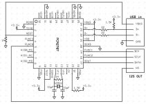
thank you Pretty obvious mistakes 
I've updated the schematic below (I can't see how to edit the first post ).
).
Do you have some experience with that chip and external clocks ? The datasheet says that :
Basically, the question is : is the SPACT system really good enough to provide a decent clock or should I try to implement a XO clock on it ?
Pretty obvious mistakes I've updated the schematic below (I can't see how to edit the first post
).Do you have some experience with that chip and external clocks ? The datasheet says that :
An external clock can be supplied from XTI (pin 28 for PCM2704/5, pin 12 for PCM2706/7). If an external clock is supplied, XTO (pin 1 for PCM2704/5, pin 13 for PCM2706/7) must be left open. Because no clock disabling pin is provided, it is not recommended to use the external clock supply. SSPND (pin 27 for PCM2704/5, pin 11 for PCM2706/7) is unable to use clock disabling.
Basically, the question is : is the SPACT system really good enough to provide a decent clock or should I try to implement a XO clock on it ?
Attachments
No point to do it. You 'll not improve nothing. SPACT system has own VCO, which determine phase noise level of the output clock. XTAL clock only provide functionality of SPACT system, but it is not reference signal of SPACT. Phase random walks, which depend by jitter of XTAL clock, has enough high frequency spectrum to be eliminated by analog PLL, which followed after SPACT.
00940, are you designing a higher end USB dac? I have built your 2702 USB dac and have been impressed with it, but I am interested in pushing the envelope to see what can be done with a 2707> I2S >pcm1798. I am still wating on my 2707 sample to ship. Is it time to start a new thread for a USB super DAC?
Niles
Niles
http://www6.head-fi.org/forums/showthread.php?p=982018#post982018
We're discussing here a DAC based on the PCM2707, followed by the PCM1794. The idea would be to have a dac based on a few boards : a rectifier/preregulator board with LM317-337 (providing +5V, +7V and +/-15V), a digital board with the chips and the final rectification and finally an output board with the output stage. I found an old post in this board, showing how BelCanto used a THS4130 differential opamp for I/V conversion in the DAC2. That could be the basis of the output stage, with an opa627 for balanced to unbalanced conversion and LPF.
We're discussing here a DAC based on the PCM2707, followed by the PCM1794. The idea would be to have a dac based on a few boards : a rectifier/preregulator board with LM317-337 (providing +5V, +7V and +/-15V), a digital board with the chips and the final rectification and finally an output board with the output stage. I found an old post in this board, showing how BelCanto used a THS4130 differential opamp for I/V conversion in the DAC2. That could be the basis of the output stage, with an opa627 for balanced to unbalanced conversion and LPF.
thanks for the link, I havent checked in on that thread in awhile. It looks like you and the others are already working out some of the same questions that I had independently arrived at. I am not registered at head-fi, so forgive me for crossing the forums for the same topic, but I still have one unanswered question. The 2707 is independently clocked from within using the SPact circuitry. However, the 1794 requires its own master clock, preferably a discrete design such as Guido's. I always was poor at timing diagrams, but it seems to me that the Data clock out of the 2707 on the I2S line needs to be synchronous with the master clock of the 1794. Is this correct, and is some glue logic going to be necessary? Anyone?
BTW, I really think that a discrete open loop I/V with a minimal gain stage is the way to go with these converters. In my mind it makes no sense to use an op-amp when it isnt a lot more difficult to use a discrete circuit. This is especially the case if your design calls for discrete boards for each functional block.
Niles
yes. Jocko's simplified circuit or a minor modification.
http://www.diyaudio.com/forums/showthread.php?s=&threadid=6121
There are some follow up posts that include schematics for some improved versions. I am a fan of minimal circuits. Some of the other participants may wish for the convenience of op-amp implemenations, and that may be the best part of your proposal to break up the function blocks. That way, we can roll our own output stage based on own needs and design philosophies.
Niles
USB DAC
Hello guys,
I recently designed a complete USB upsampling DAC for an internationally renouned audio company using similar devices to what you have discussed. Also I have done a thorough design review of the BelCanto DAC2 and this unit should by no means be used as a basis.
Assuming my estimate of what the interfacing is to the PCM1794 (I didnt use this device) your design will not work.
I2S is a packaging format and is as different from SPDIF as you could possibly get. I2S uses three signals (LRCK, BCK and DATA) the SPDIF is an embedded serial packetised protocol over a single ended medium.
Again assuming the PCM1794 doesnt accept SPDIF directly (and I'd have to look at this) you need an additional conversion stage to convert SPDIF to I2S (or RJ/LJ). Asahi Kasei/Cypress stock Digital Interface Receivers and make several variations of these.
Clocking is a pain in the a**! I ended up having 14 different clock frequencies bouncing around the board and a few crystals. This area is where you get all the problems and the most opportunity for improvement!
Likewise powersupplies are a similar pain. I designed a proprietry active noise attenuator and used multiple regulation stages. BelCanto's DAC2 is terrible in this respect, and its layout is awful.
Siimilarly their attention to clocks is also lacking, and I still have no idea why they put on a huge great CPLD/FPGA??!! It doesnt need much in the way of processing and inherent latencies of FPGA/CPLD silicon worsen the effects of jitter.
There is nothing wrong with the analog output stage example given in the app notes. Instrumentation amplifiers produce considerably less noise, but the specs of the devices specified are more than adequate. Just start off with a decent layout and you get similar performance gains with no additional cost (inst amps = expensive).
I have had lengthy discussions with several authorities in the field and the topology of the I/V conversion stage is a hotly contested issue. Some promote the opamp based one, others the simple resistor. I found no noticable difference between the two.
One final note... You will hear the effects of jitter, as it produces vast distortion effects, the overall THD of a 'circuit' (using low THD parts) will not be as easily detected.
Feel free to email me if you have any further questions. Just put DIYAUDIO - USB DAC in the subject so that it is spotted amongst the spam.
Have fun!
Apollyon25
You appear well meaning, so I will take a pass on the skewer here and just suggest that you actually take a look first at the entire thread posted above to the head-fi forum before sharing any more of your wisdom here. After that, you might want to look at the data sheet for the TI/BB PCM2707.
Niles
Niles
Re: USB DAC
Our big problem now is : the pcm1794 needs the classical 3 I2S signal (LRCK, BCK and DATA) and the PCM2707 is able to provide those. However, the PCM1794 also includes a digital filter. This digital filter requires a system clock. This clock needs to be synchronized with the LRCK clock. The question is : is the sck output of the PCM2707 able to provide that sck a/ synchronized, b/ with low enough jitter ?
Niles : have you considered the passlabs D1 stage ?
PCM1794 doesn't accept direct spdif. But the PCM2707 usb device is able to directly output I2S, not spdif. Why would we need another conversion ?apollyon25 said:Assuming my estimate of what the interfacing is to the PCM1794 (I didnt use this device) your design will not work.
I2S is a packaging format and is as different from SPDIF as you could possibly get. I2S uses three signals (LRCK, BCK and DATA) the SPDIF is an embedded serial packetised protocol over a single ended medium.
Again assuming the PCM1794 doesnt accept SPDIF directly (and I'd have to look at this) you need an additional conversion stage to convert SPDIF to I2S (or RJ/LJ). Asahi Kasei/Cypress stock Digital Interface Receivers and make several variations of these.
Our big problem now is : the pcm1794 needs the classical 3 I2S signal (LRCK, BCK and DATA) and the PCM2707 is able to provide those. However, the PCM1794 also includes a digital filter. This digital filter requires a system clock. This clock needs to be synchronized with the LRCK clock. The question is : is the sck output of the PCM2707 able to provide that sck a/ synchronized, b/ with low enough jitter ?
Niles : have you considered the passlabs D1 stage ?
I havent really looked at the D1 circuit yet. I would prefer to work with BJTs on this but there are other options for FET stages, such as Borbelly's. With any of them we must choose between a DC servo and AC coupling. Yet another I/V is the one in M.O Hawksford's I/V paper. Both the Borbelly and the Hawkford circuits include a servo.
What I like about Jocko's circuit and the variants put up in other threads, one of which you posted further up in this thread, is the elegant simplicity and that they are reputed to sound really good, especially compared to opamp solutions. I see on the other thread that you are considering the D1 stage. I will take a look at it.
What I like about Jocko's circuit and the variants put up in other threads, one of which you posted further up in this thread, is the elegant simplicity and that they are reputed to sound really good, especially compared to opamp solutions. I see on the other thread that you are considering the D1 stage. I will take a look at it.
soldering isn't really that bad. The pins on the pcm2707 have more space between them than on a pcm2702 or pcm1794.
The project is honnestly quite in standby. I finally won't have the time to build anything and conduct tests before next july or so. Not tomorrow as you can see. In the meantime, I'm still trying to gather as much information as possible and to optimize the layout of the prototype (and hopefully, it could be the last version). Choice on output stage is still the problem number one.
The nice thing with using the PCM1794 is the simplicity of the clok stuff. Going with tda1543 could be more tricky. The digital section as I have it on my drive looks fine and I won't probably touch it anymore. I know some won't like this thing with oversampling, digital filters and opamps but it's not intented to be more than a personnal project this time.
Why is that...I was under the impression that I2S would be all that is necessary....???Going with tda1543 could be more tricky.
I know some won't like this thing with oversampling, digital filters and opamps but it's not intented to be more than a personnal project this time.
That's what audio is all about imo...you have to design for your own ears and tastes.

Can the PCM2707 work in "slave" mode for the clock frequency? This way we could put the XO onto the DAC and let the PCM2707 send data only when it is needed.
Another question:
Do you know a link where I can find some information about how-to convert the 16-bit I2S signal to 18-bit I2S signal for AD1865?
Another question:
Do you know a link where I can find some information about how-to convert the 16-bit I2S signal to 18-bit I2S signal for AD1865?
- Status
- This old topic is closed. If you want to reopen this topic, contact a moderator using the "Report Post" button.
- Home
- Source & Line
- Digital Line Level
- PCM2707, I2S out