And in the last (?) player with 1541A, pin 4 is connected to pin 2.
That's the Marantz CD7 with the "famous" TDA1541/A/N2 (double crown). They shurely were not preparing that player for the old 1541...
And the cap is .... 680pF.
Think a 680 cap must be cheaper than a 470 cap
So one could put a 1541 in (actually two )
)
Almost one again, must go zzzzzzzzzzzz
That's the Marantz CD7 with the "famous" TDA1541/A/N2 (double crown).
They shurely were not preparing that player for the old 1541... And the cap is .... 680pF.
Think a 680 cap must be cheaper than a 470 cap
So one could put a 1541 in (actually two
)Almost one again, must go zzzzzzzzzzzz
zygibajt said:Guido,
I have just read one of your older posts when you tried to exchange older M4804A chip in your CD 650 for SAA7210.
Did SAA7210 work as a direct replacement,or there were some diffrances?
I have the player with that old chip and have some spare SAA7210 to drop in.
Bartek
Think it worked as direct drop-in. The 4804 should have faults, but in my player i did not see/hear them. But i could not see if the components around it were different than the schematics i have with the 7210 (SMD). So not fully shure. Never found anything on that chip.
But in general, if it works, don't break it

guido said:
1541: pin 4 = SCK, no DEM cap
1541A pin 4 = nothing, DEM cap.
So 1541 in 1541A player
So 1541A in 1541 player should not work, since DEM cap is not
there.
Aren't we dutch some funny guys
I have the DEM cap in my CD304mkII too, and that was made for 1541.
Maybe they knew about the coming 1541A and put the cap there for chip upgrade.
Or the datasheet is wrong and there is no internal cap in the 1541.
I asked Mr. FLUKE about capacitance on pins 16 & 17 on both chips and he said that there isn't any.
So, if there is an internal cap in the 1541, it is not connected to the pins.
Another question regarding the 7220.
In the 304 there are two smd transistors around pin 21, in the cd650 it is only one, and in the 880 there is nothing.
Same thing: All chips work in all players.
Any pinout differences with a/B version ?
I have the datasheet but can not find anything.
Sigh....do you measure other passives as well IN circuit ?Bernhard said:I asked Mr. FLUKE about capacitance on pins 16 & 17 on both chips and he said that there isn't any.
rbroer said:
Sigh....do you measure other passives as well IN circuit ?
Sure
,A 1541A on board shows something, off board nothing.
Bernhard said:
I have the DEM cap in my CD304mkII too, and that was made for 1541.
Maybe they knew about the coming 1541A and put the cap there for chip upgrade.
Or the datasheet is wrong and there is no internal cap in the 1541.
I asked Mr. FLUKE about capacitance on pins 16 & 17 on both chips and he said that there isn't any.
So, if there is an internal cap in the 1541, it is not connected to the pins.
Another question regarding the 7220.
In the 304 there are two smd transistors around pin 21, in the cd650 it is only one, and in the 880 there is nothing.
Same thing: All chips work in all players.
Any pinout differences with a/B version ?
I have the datasheet but can not find anything.
In HtP's article about DEM reclocking, he precises that in the non A version, the cap is internal but the pins are connected, so you can certainly add a cap too
Bernhard said:
Sure
A 1541A on board shows something, off board nothing.
I give up
Seems you don't care about any internal circuit inside the chip, like an emitter coupled multivibrator.
In order to measure the internal DEM capacitor of the TDA1541 you need to disconnect at least one side of it. Since it's located in the TDA1541, you better bring your microscope and tweezers


Pedja said:Henk, thanks again for your posts, I consider them very valuable.
I guess it is no problem to have the same delay for all the lines but you will not have the same delay for all the frequencies. Honestly, I do not have an idea if this could be bad or not, just want to note that the general 10ns becomes some 9.7ns on 2.8MHz and 8.6ns on 6.4MHz.
Pedja
Delay itself is not bad. The TDA1541 is an end user of the signals, it takes only some nsec more before the music reaches you. There are no set-up and hold problems in this case.
regards,
Pedja said:Henk, thanks again for your posts, I consider them very valuable.
I was not referring to the noise/resistor induced jitter, I was referring to the smoothed waveform like generally less wanted waveform here because of the problem of indeterminacy of the moment of transition in time. Attached are the bandwidth unlimited ~2.82MHz square and squares limited wit RCs of 12ns and 22ns. Are there good reasons why they usually use just square signals here or not? Or the rise time is all we need to determine the best bandwidth of these squares?
Pedja
The digital inputs of the dac form a comparator, they compare the input signal with a reference. Each comparator has an input refered noise density and a comparator noise bandwidth. The total input refered noise power is the input refered noise density integrated over the comparator noise bandwidth. The comparator noise bandwidth depends on how it is build, and how the gain vs frequency roloff is designed.
Total integrated noise power can be calculated into the input refered noise voltage.
A low comparator noise bandwidth gives a low input refered noise voltage. The relation between output slew rate and noise bandwidth is defined by the input gm over C ratio.
The noise voltage converts to time uncertenty, or jitter, with the input signals slew rate.
There are indeed reasons to use square waves, the are fast enough. But if you know the input refered noise voltage, then you can calculate the minimum required input slew rate for a given increase in jitter. If you can do this, than you can also minimize the cross talk of the digital input signals into the dac.
regards,
fine, i nearly understood this. Now could anybody please post the schematic of the circuit to get the TTL down to the desired voltages the TDA1541 likes best? And why not with an active element as a differential amp with gain < 1 so the signal would be present inverted and noninverted to feed 2 DACs for balanced operation?
till said:And why not with an active element as a differential amp with gain < 1 so the signal would be present inverted and noninverted to feed 2 DACs for balanced operation?
I do not consider that as a good idea. Tomorrow I will receive the SN74HC86N exclusive or logic chips and I will play with the 2 TDA1541A you kindly send to me some time ago for a balanced operation . See the D1 schematich just before the PCM63 to know what I am thinkin. There , four EX OR ar used as buffer and as inverter for DATA in one chip.
The output stage will be D1 without buffer. I am expectin' good results.
Thanks
I stated:
Current reference generator for the output current is between -5V and -15V. Output current from the dac comes out of pin 6, 25 via diode switches or comes out via the +5V pin 28 by darlingtons. This means that complementory output signals L+R flow in supply pin 28.
And Pedja responded:
I do not quite figure this. Three or 4 active divider pins are inside -15V- -5V range but the others are not.
Interesting note about pin 28.
Pedja
I made two statements.
1. Current reference generator for the output current is between -5V and -15V.
What was ment here is where the current 'reference' generator circuit is, that it is supplied between the -5V and the -15V pins. With other words, the supply voltage of the current reference is 10V. This current reference is the reference for all binary weigthed currents in the TDA1541(A). The supply rejection ratio for this current reference is not infinite, thus this 10V should be as constant as possible.
The binary weigthed currents in the TDA1541(A) are made accurate by the dem circuit, the voltages on the filters for this dem circuit are not direct related with the supply voltage of the current reference. The fact that (some of) these voltages are above the supply voltage of the current reference is not in conflict with my statement.
2. Output currents from the dac comes out of pin 6, 25 via diode switches or comes out via the +5V pin 28 by darlingtons. This means that complementory output signals L+R flow in supply pin 28.
The inner curcuit of the dac can be seen as a binairy controlled differential stage.
One output (the not used) flows in pin 28, thus +5V. The outher output in pin 6, 25. The sum of signal currents in pin 6, 25 and pin 28 is constant. That means that it is advantageous to bring the output currents in pin 6, 25 back into the +5V supply. That can be done by e.g copying the output current into the +5V supply. If done correct, the signal in the +5V decoupling capacitor completely disapears.
regards,
This leads mo to the conclusion a local decoupling between the pin 15 (-15V) and the pin 26 (-5V) could be welcome.
Also, putting aside the last possibility you mentioned, the pin 28 (+5V) should have nice AC path to the analog ground.
However, with existing decoupling of all the rails to ground and decoupling directly between +5V and -5V things are becoming a bit horrible.
Btw, it is not that I am asking for proofs but I am curious about the source of your info about 1541. Is it someone involved in the designing of this chip? Finally, I see you are in Eindhoven, maybe this means something?
To clarify/confirm the things spoken earlier, a low passing of the I2S lines is conventionally done using series resistors and capacitance of the inputs, but did I understand you, do you consider the shunting of HF current to the (digital) ground instead to the substrate as qualitatively significantly different thing?
Thanks,
Pedja
till said:fine, i nearly understood this. Now could anybody please post the schematic of the circuit to get the TTL down to the desired voltages the TDA1541 likes best?
Oh yes, please
Pedja said:
Btw, it is not that I am asking for proofs but I am curious about the source of your info about 1541. Is it someone involved in the designing of this chip? Finally, I see you are in Eindhoven, maybe this means something?
Thanks,
Pedja
Yes, yes.
Pedja said:
To clarify/confirm the things spoken earlier, a low passing of the I2S lines is conventionally done using series resistors and capacitance of the inputs, but did I understand you, do you consider the shunting of HF current to the (digital) ground instead to the substrate as qualitatively significantly different thing?
Thanks,
Pedja
Yes, it keeps the hf currents out of the chip.
regards,
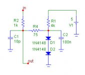
Bernhard said:Is this schematic ok ? Swings from 0,9V to 1,6V.
With R4 = 75 ohm, time constant is only 750psec. So R4 = 1k will give a time constant of 10nsec. For R1 I propose 4k7 with 5V logic input or 3k3 with 3V logic input. This will also reduce the load of the logic. It assures also that there is always current in the diodes.
I would prefer to use this circuit three times, for DATA, BCK and WS each. This avoids data dependence of slicing levels.
regards,
- Status
- This old topic is closed. If you want to reopen this topic, contact a moderator using the "Report Post" button.
- Home
- Source & Line
- Digital Line Level
- TDA1541 info