Bernhard said:Never heard that rising time of logic input can be too high.
Only about problems if they are too slow.
Logics have a L to H switching point like 3,5V and H to L like 1,5V for best noise immunity.
Hi,
rising time is too FAST.
And the for the TDA it appears to be: low=1.2, high is 1.4 volt.
Pedja,
In the datasheet all three supply voltages are stated with their supply voltage ripple rejection. Does this not state that they are all three used for the analog output ??

mvg,
guido said:
And the for the TDA it appears to be: low=1.2, high is 1.4 volt.
Oops, low=1.3, high=1.5

And do you have an idea how to convert 0-5 to 1.3-1.5 (or 1.2-1.6)?
I tried to do somethink with 3 resistors (a series resistor, one from Vcc and one from GND), but this won't work, and would draw way too much currenta
so you formed a voltage divider for about the middle of the 2 voltages desired and tried to modulate this middle point with the signal.
what about between the two resistors forming the voltage divider a transistor. the transistor is biased so it is about open, the voltage divider shows one of the both voltages we need. and the base the the signal is modulating the transistor.
This could also make a fine circuit to feed an inverted and a noninverted signal without time difference into balanced DAC. One taken at emitter, one at collector.
rising time is too FAST.
yea, but the big question is: in what way should that take effect on the DAC? (sound like blue led sound)
Should be easy enough to put a resistor + capacitor in the signal line.
guido said:rising time is too FAST.
And the for the TDA it appears to be: low=1.2, high is 1.4 volt.
Rising time of what chip ?
Signal swing is between 1,2 and 1,4 V ?

Datasheet say it is TTL compatible.
Hmmm, funnily enough, it does.guido said:In the datasheet all three supply voltages are stated with their supply voltage ripple rejection. Does this not state that they are all three used for the analog output ??
Though the numbers tell that -15V is the real analog supply, +5V is notably less analog supply and -5V is even more less analog supply (maybe crosstalk? <- joke).
I think I will proceed to threat them like before.
Fine with me.I think we should cook up a circuit and just try it. If it works, great.
If it does not improve the sound, we just forget about it.
Pedja
I should look better when I am linking something. It is not the post that I wanted to refer to, actually the sentence I quoted (“*low* frequency rolloff) is ambiguous and in one sense perfectly applies if you understand it as lpf with too low roll-off frequency. Unfortunately I can not find the post I had on my mind (it was IIRC wildmonkeysects’s one), I’ll post the link if I find it. Sorry.Pedja said:“A significant factor is the *low* frequency rolloff of the transmission medium shifting the level of the transition points.”
http://www.audioasylum.com/audio/tweaks/messages/30411.html
till said:
so you formed a voltage divider for about the middle of the 2 voltages desired and tried to modulate this middle point with the signal.
what about between the two resistors forming the voltage divider a transistor. the transistor is biased so it is about open, the voltage divider shows one of the both voltages we need. and the base the the signal is modulating the transistor.
This could also make a fine circuit to feed an inverted and a noninverted signal without time difference into balanced DAC. One taken at emitter, one at collector.
I'll try this
One solution I was thinking about was to use a transformer, and place the output 2 diodes drops above ground.
The digital inputs of the TDA1541(A)
The digital inputs are pnp differential stages, the reference voltage made by two forward biased diodes. this gives a reference voltage of about 1.4V. you can measure this your self by measuring the change in current of the digital inputs as function of input voltage. The input current will be half if the input stage is at ballance.
Reqiured swing for this input stage is 200mVpp around bias, for safety 400mVpp.
The base of a pnp in this bipolar process is juction isolated to the substrate, the input capacitance is therefore mainly to the substrate. Fast and large digital input signals cause capacitive currents in the substrate. Thes can be lowered by making the input signal not larger and not faster than needed.
Thus not larger than 400mVpp around bias.
Not faster than 10 to 30nsec rise time. This rise time is already faster than required is the ft of the pnp is taken in acount. A lateral pnp is in this process not faster than 10MHz, a vertical pnp slightly faster.
You can make these signals with a resitive divider from your digital source to a bias voltage of also two forward biased diodes. Use 1 mA in the diodes. Reduce the speed og the input signal for the TDA1541(A) with a capacitor of say 10pf, to digital ground. Make this circuit separate for each active input.
Do not use transformers or active circuitry, this will cause data dependency of the delay.
Please take notice that pasive delay itself does not cause jitter.
Please take notice that if the input rise time is fast enough, no additional jitter is introduced.
regards,
Hi,
I already had the impression you were reading this... .
Thanx for taking over!
Could you also make some more statements on the +5 and -5 supplies? And decoupling between -5 and +5? Easier doing it here than me copying answers etc..
Thanks for your patience on answering my mails (>10) and replying to my criticial mails

I already had the impression you were reading this...
.Thanx for taking over!
Could you also make some more statements on the +5 and -5 supplies? And decoupling between -5 and +5? Easier doing it here than me copying answers etc..
Thanks for your patience on answering my mails (>10) and replying to my criticial mails
Henk, thanks for the input.
What you are suggesting (10-20ns) will move the waveforms (especially BCK) toward the sinewaves and the transition points will become less defined. This leads to jitter as far as I know. Though it still can be acceptable in non-o/s applications.
If you can shed more light on for what in the analog part are used +5V and -5V supplies, it will be more than welcome.
Pedja
Pedja
1. Delay is not important as long as the delay is equal for all inputs.
2. Delay has no influence on the definition of the transition as long as the noise of the delay element or the noise of the inputstage does not significantly cause jitter.
3. The noise bandwidth of the pnp input stage is less than 5MHz, the noise density of the input stage is far below 1k. The resulting integrated noise is far below that for the input filter.
3. Maximum specified input rise time is 35nsec for all applications.
4. An input RC filter with R = 1k and C = 10pf has a bandwidth of 15MHz. The noise of this resistor in that bandwidth becomes 0.13nV/sqrtHz * sqrt(1k * 15MHz) = 16microVolt. If the RC filter is driven such that the output voltage equals 400mVpp, the slew rate at 200mV will be 50nsec/V.
The resultant jitter will be 16microVolt * 50nsec/V = 800femtoSeconds or 0.8psec rms.
This will cause noise which is .8psec/22.67usec or -149dB down wrt full scale.
I think this can be accepted.
regards,
What you are suggesting (10-20ns) will move the waveforms (especially BCK) toward the sinewaves and the transition points will become less defined. This leads to jitter as far as I know. Though it still can be acceptable in non-o/s applications.
1. Delay is not important as long as the delay is equal for all inputs.
2. Delay has no influence on the definition of the transition as long as the noise of the delay element or the noise of the inputstage does not significantly cause jitter.
3. The noise bandwidth of the pnp input stage is less than 5MHz, the noise density of the input stage is far below 1k. The resulting integrated noise is far below that for the input filter.
3. Maximum specified input rise time is 35nsec for all applications.
4. An input RC filter with R = 1k and C = 10pf has a bandwidth of 15MHz. The noise of this resistor in that bandwidth becomes 0.13nV/sqrtHz * sqrt(1k * 15MHz) = 16microVolt. If the RC filter is driven such that the output voltage equals 400mVpp, the slew rate at 200mV will be 50nsec/V.
The resultant jitter will be 16microVolt * 50nsec/V = 800femtoSeconds or 0.8psec rms.
This will cause noise which is .8psec/22.67usec or -149dB down wrt full scale.
I think this can be accepted.
regards,
Henk, I hope you have some hints about that
On another topic (http://www.diyaudio.com/forums/showthread.php?postid=370006#post370006 ) stefanobilliani was talking about pin4 being a (11.xxxx MHz) input. In fact he was "wrong" because he was reffering to the TDA1541 (non-A) datasheet.
I wouldn't be surprised if this is still activated on the TDA1541A, but just undocumented.
Do you know something about that?
Stefanobilliani was talking about pin4 being a (11.xxxx MHz) input. In fact he was "wrong" because he was reffering to the TDA1541 (non-A) datasheet.
I wouldn't be surprised if this is still activated on the TDA1541A, but just undocumented.
Do you know something about that?
Pin 4 is activated on the TDA1541A.
regards,
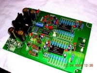
Tda1541a info
hi,
if U want TDA1541a info.pls email to me to collect the PDF file.
this is my new design which use parallel (two) tda1541a NOS.
DAC with CS8414 contain I2S (SYN-SCK-SDATA) & CS8412/8414 can run use dip.switch setting for syn mode or aysyn mode.
thanks
thomas
www.diyaudiocraft.com
hi,
if U want TDA1541a info.pls email to me to collect the PDF file.
this is my new design which use parallel (two) tda1541a NOS.
DAC with CS8414 contain I2S (SYN-SCK-SDATA) & CS8412/8414 can run use dip.switch setting for syn mode or aysyn mode.
thanks
thomas
www.diyaudiocraft.com
Attachments

Pedja said:Henk, thanks for the input.
If you can shed more light on for what in the analog part are used +5V and -5V supplies, it will be more than welcome.
Pedja
Logic in the TDA1541(A) is current routing logic, in general between the -5V and the +5V pins. The logic swing is some hundreds of millivolts. Supply current is nearly constant, only a very small capacitive spike flows into the substrate.
Current reference generator for the output current is between -5V and -15V. Output current from the dac comes out of pin 6, 25 via diode switches or comes out via the +5V pin 28 by darlingtons. This means that complementory output signals L+R flow in supply pin 28.
regards,
HtP said:
Pin 4 is activated on the TDA1541A.
regards,
Could you give us some more details?
I know that pin4 is activated in the TDA1541A, since it is the right channel digital input, when set up in simultaneous mode.
What I wanted to know, is if the pin4 can be used as a SCK input when the DAC is set up in I2S mode.
Thanks
Alex
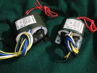
Tda1541a info
hi Bernhard,
very thanks for your comment.
this circuit was one of Germany friend send to me & I reference several more then Layout the PCB.
http://hjem.get2net.dk/torbenk/dualdactube.htm
http://users.podolsk.ru/boga/DAC.html
http://www.ndh.net/home/kboehm/T-DAC-P2.htm
Sorry I had a little misunderstanding that
the I2S lead out can used for several purpose. one of the purpose was for the coming re-clocking parts.
But some of the diyer not like it. So I setting for options.
This several days I was testing this PCB & testing the Power transformers.
I collect this which prepare for this PCB & the output stage which use 6X4/diode with 6C45,EC88,EC86,EC8010 or 6DJ8 SRPP circuit. Also, I had another test need to test is, if the user use 6C45 or EC8010. Then use the pre-amp output 10K:600ohm to output.
I don't know the performance but i will test in detail.
pls see the power transformers.
thanks
thomas
hi Bernhard,
very thanks for your comment.
this circuit was one of Germany friend send to me & I reference several more then Layout the PCB.
http://hjem.get2net.dk/torbenk/dualdactube.htm
http://users.podolsk.ru/boga/DAC.html
http://www.ndh.net/home/kboehm/T-DAC-P2.htm
Sorry I had a little misunderstanding that
better wait what comes out from the low voltage I2S signal swing thread
the I2S lead out can used for several purpose. one of the purpose was for the coming re-clocking parts.
But some of the diyer not like it. So I setting for options.
This several days I was testing this PCB & testing the Power transformers.
I collect this which prepare for this PCB & the output stage which use 6X4/diode with 6C45,EC88,EC86,EC8010 or 6DJ8 SRPP circuit. Also, I had another test need to test is, if the user use 6C45 or EC8010. Then use the pre-amp output 10K:600ohm to output.
I don't know the performance but i will test in detail.
pls see the power transformers.
thanks
thomas
Attachments
Bricolo said:
What I wanted to know, is if the pin4 can be used as a SCK input when the DAC is set up in I2S mode.
Thanks
Alex
As far as I know, yes, but the designer told me that it was not (longer) needed. I have no experience with it.
regards,
- Status
- This old topic is closed. If you want to reopen this topic, contact a moderator using the "Report Post" button.
- Home
- Source & Line
- Digital Line Level
- TDA1541 info