Thanks!
"Very often the groundplane is intersected by a slot, between the analogue and digital part of the PCB. The two planes are then connected beneath the AD or DA converter chip, or even worse at the supply-lines entry on the PCB (as advised by some IC manufacturers). With the planes separated, signal currents that cross the intersection are forced to return via the groundplane and as such need to describe a huge loop, around the intersection."
One thing I do not understand: what type of signal currents want crossing the intersection, if I have a saparate analog and digital PSU (tranformer too)??
Lots of capacitive hash from the digital side, the currents needed to charge and discharge the gates of the switches in the DAC need to get back to the digital side somehow.
An important note on DAC and (especially) ADC parts, they often have pins labelled as AGND and DGND, this is NOT an invitation to route them to separate plains, they should be connected to a common plane! The reason for the separate pins is to avoid common impedance coupling in the pin and bond wire within the package.
Also on ADCs of the usual charge transfer type, that few nF cap right by the analogue input pins is operating as an RF part, keep it physically as small as possible and keep the loop area tiny.
The other trap with slotted planes is that any trace that crosses the slot defines a bigger then needed loop area, because the return current must flow around the slot.
On power decoupling, you actually really do not want too much Q, and fitting a few ohms of Q killing resistor between the rails and each of those decoupling networks really would not have hurt anything. The reason is that a long power trace can have a surprising amount of inductance and if you add too much modern low ESR electrolytic, can actually acquire resonances in the ultrasonic or even in the audio band, run the numbers with say 10,000uf and modern polymer sorts of ESRs and ESLs sometime it is quite instructive. Low ESR is not always a win when combined with the ESL of the cap and trace, some Q killing series resistance can be most helpful.
Regards, Dan.
Thanks!
"Very often the groundplane is intersected by a slot, between the analogue and digital part of the PCB. The two planes are then connected beneath the AD or DA converter chip, or even worse at the supply-lines entry on the PCB (as advised by some IC manufacturers). With the planes separated, signal currents that cross the intersection are forced to return via the groundplane and as such need to describe a huge loop, around the intersection."
One thing I do not understand: what type of signal currents want crossing the intersection, if I have a saparate analog and digital PSU (tranformer too)??
Think of it this way: The high-frequency current transients always want to return on the ground-plane directly under the trace. If you break that ground-plane, you are forcing these currents to take another path, less optimum.
Low-frequency currents will always take the path of least resistance, a direct line, or as they say "as the crow flies".
Therefore, the best scenario is if the path of least resistance and the ground-plane under the trace are one and the same.
Steve N.
Empirical Audio
Lots of capacitive hash from the digital side, the currents needed to charge and discharge the gates of the switches in the DAC need to get back to the digital side somehow.
An important note on DAC and (especially) ADC parts, they often have pins labelled as AGND and DGND, this is NOT an invitation to route them to separate plains, they should be connected to a common plane! The reason for the separate pins is to avoid common impedance coupling in the pin and bond wire within the package.
It is okay to have a digital and an analog plane, but connect them with a wide strip under the D/A chip. IF you do this, however, you must be careful how you earth-ground the circuit. It is easy to incidentally force ground-loop noise to flow across this high-impedance link and get a voltage drop and therefore noise as a result. Been there, done that.
On power decoupling, you actually really do not want too much Q, and fitting a few ohms of Q killing resistor between the rails and each of those decoupling networks really would not have hurt anything. The reason is that a long power trace can have a surprising amount of inductance and if you add too much modern low ESR electrolytic, can actually acquire resonances in the ultrasonic or even in the audio band, run the numbers with say 10,000uf and modern polymer sorts of ESRs and ESLs sometime it is quite instructive. Low ESR is not always a win when combined with the ESL of the cap and trace, some Q killing series resistance can be most helpful.
This depends on where you locate the decoupling caps and the sizes. If HF caps are close to the loads, there will be no resonant issue.
Steve N.
Empirical Audio
I personally don't like WIMA. There are other better film caps. I'll let you find them...
Steve N.
Empirical Audio
Panasonic ECW?
You might want to read this pdf, post 3. Pretty much a very good guideline for PCB layout in general.
PCB Layout Process and Guidelines?
PCB Layout Process and Guidelines?
I would think that things like oscillators would produce the most amount of disturbances.
I have seen ferrite beads used on the supply to this portion to help keep the noise isolated.
The polymer capacitors on digital supplies work great, however, I try to adhere to using close to the same esr as the electrolytic part would have had in order to avoid resonance. Using a 47uf polymer part as close to the load (DAC)as possible without any tiny ceramic parts has worked well.
Not a layout specific comment, but just something to consider maybe. I would do as others have mentioned and focus on the grounds, keeping it tight. Maybe to study some of the data sheets to see how the recommended layouts appear. I have noticed that the power and clock pins are usually not near the signal pins, the traces would likely follow suit.
Last edited:
I would think that things like oscillators would produce the most amount of disturbances.
I have seen ferrite beads used on the supply to this portion to help keep the noise isolated.
Not unless you want higher jitter from those oscillators. By doing this, you are increasing inductance from the power source and thereby decreasing di/dt that the oscillator needs.
Steve N.
Empirical Audio
I would think that things like oscillators would produce the most amount of disturbances.
I have seen ferrite beads used on the supply to this portion to help keep the noise isolated.
It depends on the frequency to what extent those disturbances do harm. Sigma-delta based DACs are sensitive to interference at all frequencies except exact multiples of their sample rate (those can at most produce a small DC offset). Some types are particularly sensitive to interferences around odd multiples of half their sample rate.
So if the oscillator produces the sample clock of the sigma-delta, you don't need to worry about its signal ending up at the wrong place in the DAC, but you do have to worry about digital signals coupling into the oscillator and affecting its jitter. If the oscillator produces any other frequency, you have to keep it from coupling into the reference and clock of the DAC.
Not unless you want higher jitter from those oscillators. By doing this, you are increasing inductance from the power source and thereby decreasing di/dt that the oscillator needs.
Steve N.
Empirical Audio
That's why you normally use a ferrite bead and a local decoupling capacitor, not just a bead.
Where I have observed this, the ferrite has been fairly large for the relatively low current operation of the clock. This was also on some pretty low $ implementations, where it wouldn’t have been done if it hadn’t produced a result.
Another trick I have seen that is more within the topic of layout, is using a healthy slot on four sides of the clock mounting. I am not sure how effective this is since frp board material is fairly rigid. I would think a more creative method of decoupling the buzz from the rest of the board could be accomplished. Maybe raised up and attached to some commonly available pins, or?
I have seen 1m resistors placed across incoming power on dac chips, but am not sure if it was just to improve the chances of not being destroyed by an esd event, or if there was some manner of damping to be gained.
Where I have observed this, the ferrite has been fairly large for the relatively low current operation of the clock. This was also on some pretty low $ implementations, where it wouldn’t have been done if it hadn’t produced a result.
I'm sure the ferrite is there for a reason, but the reason could well be to keep the clock signal clean or simply to pass EMC tests.
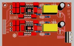
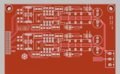
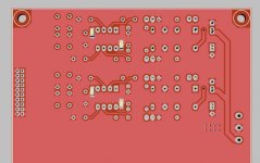
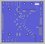
So, I've decided completly redesign my PCBs, as mentioned. I'll leaved the stacked layout and made a side-by-side arrangement with 2x 10x10cm 2 layer boards for DAC and output filtering.
First I've designed the filter PCB, it's the easiest... The to boards will be connected directly with 2 pcs. of angle 2x10 pole 2mm pin headers.
(the other 4 channels on the lower side will be simply mirrored...)
First I've designed the filter PCB, it's the easiest... The to boards will be connected directly with 2 pcs. of angle 2x10 pole 2mm pin headers.
(the other 4 channels on the lower side will be simply mirrored...)
Attachments
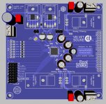
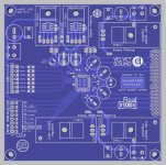
I've completly redesignd the DAC board too, see pictures...
I made the bottom GND layer as solid as possilbe, and placed the bypass capacitors on the top as near to the IC as I could. I used 0603 size SMD patterns, I'm curious how I'll to solder them...")
The drawback is that the signal paths are a little bit longer, and I must make some power bridges on the bottom. But I think these are acceptable compromisses.
Some idea to improving?
I made the bottom GND layer as solid as possilbe, and placed the bypass capacitors on the top as near to the IC as I could. I used 0603 size SMD patterns, I'm curious how I'll to solder them...
The drawback is that the signal paths are a little bit longer, and I must make some power bridges on the bottom. But I think these are acceptable compromisses.
Some idea to improving?
Attachments
I have some 10uF OsCon SMD caps for that purpose. Should I use bigger (e.g. 0805) ceramic caps?
For the analog side I'd like 10uF Elna Silmic II caps. My shunt regulators are stable by >=100nF, but too big caps would degrade the characteristic.
How do you check these resonances? Simply with an oscilloscope?
For the analog side I'd like 10uF Elna Silmic II caps. My shunt regulators are stable by >=100nF, but too big caps would degrade the characteristic.
How do you check these resonances? Simply with an oscilloscope?
Last edited:
- Status
- This old topic is closed. If you want to reopen this topic, contact a moderator using the "Report Post" button.
- Home
- Source & Line
- Digital Line Level
- General DAC design rules, layout techniques, etc.