Multi-cb also offerings via filling (so nice to place vias in SMD pads), this helps a lot; I don´t know the costs.
"Multi-cb" is very expensive for me, I do not give out 80-100€ for a bare PCB...
(I will order from PCBway, China: 100x100mm, 2 layers, 10 pieces costs 5$+25$ shipping!!)
Last edited:
@zarandok
Next time, please compare apples with apples! Ask PCBWay for 4 layers and via filling and compare.
PCBWay is very cheap for series, dimensions and standard job; its another story if you want something special.
BTW, I´m very happy with PCBWay´s work and quality and definitively recommended.
Good luck!
JP
My 2 cents,not design more of practical matter...
use 44.1/48k parts ,there is very little music at over 16 bits and 44.1k.....
So cheap out on dacs , saved money put in better analog part of circuit..
I do not understand you, sorry.
@zarandok
Next time, please compare apples with apples! Ask PCBWay for 4 layers and via filling and compare.
JP
You have right, but 80€ / PCB for a hobbist is a little too much...
How thick Cu layer is optimal for DACs? 1-2-3... oz? Is 1oz to assume?
My 2 cents,not design more of practical matter...
use 44.1/48k parts ,there is very little music at over 16 bits and 44.1k.....
So cheap out on dacs , saved money put in better analog part of circuit..
You got a point there!
btw: the signature link don't load - server cant be found...
//
Server offline for now, i hope to fix that in next month...
I simply state what i found in my humble experiments...
@zarandok i simply state that there is no need designing around expensive lets say 384k 24bit chip when you will end up playing 44.1k 16bit files at best.. So my approach is using "low" end dacs but make vert good analog part of circuit or ading balanced output, something that will produce better resaults in real everyday use..
1oz copper is standard and fine for everything except very high current use (You will know if you need it), or really fine pitch stuff (Same comment).
Filled vias are wonderful when you are working with a 0.5mm pitch BGA on a HDI board but add a stupid amount of cost to prototypes, and basically nothing audio needs it.
Samtec are fine is slightly expensive, my point on connectors was really that there are much better and denser options for board to board then 0.1 inch headers, to the point that you seldom see .1 inch connectors on modern professional boards except possibly where ribbon cable is in play.
It is true that there is seldom much point in making one part of a system orders of magnitude better then the surrounding electronics, measure then improve the worst bits, and repeat!
Regards, Dan.
We all agree that PCB is an active part of an electronic card.
A DAC electronic card includes a digital part and an analog part.
Handling MHz in the digital part we need to use high speed design rules.
You want standard two layer PCB: 1.6mm, 35µm CU on both side. Don´t forget the ratio between CU thickness and trace width or via drilling.
You can find here a nice tool: Saturn PCB Toolkit - Saturn PCB Design
@zarandok
Are you an experienced layout designer (NF audio, analog and digital power supplies, RF, High Speed)?
Here an interesting link to see what is to avoid designing DAC PCB (and a lot of interesting things); go to DAC Geek Pulse part:
Au pays du grand n’importe quoi en audio, deux rencontres. | Jipihorn's Blog
@dmills
For 0.5mm pitch BGA I would use microvias and SBU technologies, perhaps filled vias for power.
A lot of designers are placing in purely NF audio designs vias directly into SMD pads to generate a THT component from a SMD component and this is not a problem if you´re manually soldering each board. NOGO if using solder paste. I´m sure if PCB´s manufacturer offering this technologie for free, a lot of board developper will use this possibilities (principally for better power decoupling while reducing distance between cap and pad). Also in audio! But you´re right, a good layout can be achieved without filled vias. But if the demand grows then the price sinks.
JP
I'am considering 4-layers but it is not so easy. Nr.1: never done before. Nr.2: I must buy a layout software. Nr.3: manufacturing costs more, if I'd like to order 1-2 pieces (only for me).
Regarding point 2, KiCAD is for free and can be used for four-layer boards; I designed the four-layer boards of my hobby DACs with it. KiCAD takes some getting used to and via stitching is a bit clumsy, but it is really a very decent layout program. I definitely prefer it over Eagle - with Eagle you can very easily generate netlists that don't correspond to the schematic you see on the screen, with KiCAD I've never had anything like that happen to me.
I've tryed KiCAD but it is not my software. If somebody is beginning to get to know a layout editor and building up new database than possibly ok, but for me it is very strange and confusing...
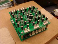
Just an example where this stacked boadrs idea comes from, see pics. The pin header must be relative massive if I want to connect two boards with about 2cm distance. Other argument for the 0,1" headers, that I can sneak through the pins with ground filling, in case of 2 layers it is very important. But I'm considering a flexible connection too instead of stiff headers...
I think the JP3 is the GND connection between the boards.
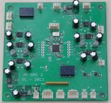
This is an ES9016 board, but I do not want to make an ESS DAC from several reasons... AK4458 is just good or better...")
Just an example where this stacked boadrs idea comes from, see pics. The pin header must be relative massive if I want to connect two boards with about 2cm distance. Other argument for the 0,1" headers, that I can sneak through the pins with ground filling, in case of 2 layers it is very important. But I'm considering a flexible connection too instead of stiff headers...
I think the JP3 is the GND connection between the boards.
This is an ES9016 board, but I do not want to make an ESS DAC from several reasons... AK4458 is just good or better...
Attachments
Last edited:
A way to minimize the loop on two layers board is to use a small ground pour on the top layer to which both the decoupling caps and the IC connect and then stitch that to a bottom layer groundplane with multiple via.- ground connenction of bypass caps (bigger electorites and small ceramics): simply to common ground pour or preferred a star grounding terminology?
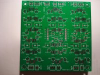
This pcb is far from perfect but it illustrates the technique.
Yep, hierarchical grounds can work but they tend to take some consideration in design to get right.
Someone got a little carried away with electrolytic decoupling caps methinks on that stacked board set, I figure that with better layout and C0G instead of those film caps I could probably get the whole thing on one board (Possibly even one eurocard) with better signal integrity.
Two layers is a massive compromise for anything non trivial, and seriously four layers does not add that much cost compared to the time saved on layout.
If you are dead set on sticking with .1 inch connectors, at least make them double row and use the second row for ground, that also makes testing much easier as you can use an IDC ribbon between the boards.
Regards, Dan.
Someone got a little carried away with electrolytic decoupling caps methinks on that stacked board set, I figure that with better layout and C0G instead of those film caps I could probably get the whole thing on one board (Possibly even one eurocard) with better signal integrity..
There are really a lot of electrolytics...
But for signal filtering I would use only good foil caps (e.g Wima FKP). For OPAs DIP-8 type (because of compatibility and interchaneablility). This allows that signal integrity of course not possible...
I'am thinking anyway to leave this stacked arrangement and make a whole new concept. Does it makes a real sense to place the first pole on the DAC board (red circle on the pic) and the other components on the other pcb next to that? Any disadvantages?
Attachments
Whats wrong with C0G? They are available these days in values useful for audio filtering which generally did not used to be the case, and are more or less blameless, I would take them over film wherever the values worked.
Incidentally, you can get SMT film caps, they are a bit of a pain and I generally try to design them out because they impose a rather too tight reflow thermal profile when using lead free, but they do exist.
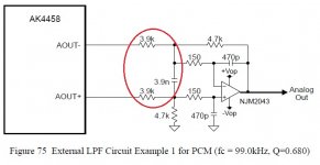
I wouldn't bother with splitting up that rather weird filter, it clearly does nothing very useful with common mode noise at the output of the DAC, relying instead on the opamps PSRR (What PSRR at a few MHz?)...
Regards, Dan.
Incidentally, you can get SMT film caps, they are a bit of a pain and I generally try to design them out because they impose a rather too tight reflow thermal profile when using lead free, but they do exist.
I wouldn't bother with splitting up that rather weird filter, it clearly does nothing very useful with common mode noise at the output of the DAC, relying instead on the opamps PSRR (What PSRR at a few MHz?)...
Regards, Dan.
I've tryed KiCAD but it is not my software. If somebody is beginning to get to know a layout editor and building up new database than possibly ok, but for me it is very strange and confusing...
Just an example where this stacked boadrs idea comes from, see pics. The pin header must be relative massive if I want to connect two boards with about 2cm distance. Other argument for the 0,1" headers, that I can sneak through the pins with ground filling, in case of 2 layers it is very important. But I'm considering a flexible connection too instead of stiff headers...
I think the JP3 is the GND connection between the boards.
This is an ES9016 board, but I do not want to make an ESS DAC from several reasons... AK4458 is just good or better...
I agree with your use of smaller electrolytic caps and particularly your use of polystyrenes. The values and locations of these are really important, so do some experimentation. As mentioned, you also need some film caps of the optimum values. It takes some experience to determine the optimum values.
I would highly recommend getting a good quality LCR meter and test the "Q" of each of the caps you are using. I like the Agilent, but it's $4K at least. Maybe a used one? Test different brands until you find the magic combination of electrolytic, film and polystyrene, all with high-Q.
Steve N.
Empirical Audio
There are really a lot of electrolytics...
But for signal filtering I would use only good foil caps (e.g Wima FKP). For OPAs DIP-8 type (because of compatibility and interchaneablility). This allows that signal integrity of course not possible...
I'am thinking anyway to leave this stacked arrangement and make a whole new concept. Does it makes a real sense to place the first pole on the DAC board (red circle on the pic) and the other components on the other pcb next to that? Any disadvantages?
I personally don't like WIMA. There are other better film caps. I'll let you find them...
Steve N.
Empirical Audio
Whats wrong with C0G? They are available these days in values useful for audio filtering which generally did not used to be the case, and are more or less blameless, I would take them over film wherever the values worked.
+1 for C0G. I've a book of E24 values going from 0.5 to 200pF in 0603. Cost was peanuts on Taobao. Tolerances aren't tight (5%) but the compact size means its simple to adjust values by measurement and paralleling - C0G's top-notch tempco and stability means the adjusted values will 'stay put'.
- Status
- This old topic is closed. If you want to reopen this topic, contact a moderator using the "Report Post" button.
- Home
- Source & Line
- Digital Line Level
- General DAC design rules, layout techniques, etc.