Regarding AVCC current and opamps, the Q2M is a mobile chip that runs at fairly low current.
Regarding overall current usage, the DAC itself and all the supporting digital circuitry runs entirely off the positive incoming supply. The negative voltage rail is only used for the output stage opamps (and to bias the AVCC opamps if used, but their output current is all positive.)
To your point though, I haven't measured AVCC current myself and particularly under maximum power conditions. Probably a worthwhile exercise for somebody to do. AD797 might be a safer bet for AVCC power if more current capability is desired without measuring.
Now that you have me thinking more about it I am inclined to measure it but too busy with other things to get to it for awhile.
Last edited:
Hi Markw4,
I own a blue pcb version that works, sound flat (as user sbf2 said on post 162), and come without 1.2v regulator from factory, same with a different blue version of a friend, looking to the chinese seller pictures seems that v1.07 is build in the same way, that is why I´ve asked, looks odd...
Just received my board and its Ver1.07. and I can confirm that the 1.2v reg is missing as borlix reports.
Is it an improvement or a cost cutting exercise?
Attachments
Regarding the regulator, have you measured the voltage there? If it looks right it probably is right, is all I can say. Still don't know why some boards had regulators and some not. Perhaps information or advice from ESS has changed over time, but that is entirely speculation on my part.
Back to the issue of AVCC current for a moment. ESS does say something about that which I am not at liberty to talk about. Maybe I could say it is suggestive the schematics on their downloads page are probably still good, maybe with some variation depending on particular operating conditions. Bottom line: I am not worried but still plan to do a measurement to see for myself when time is available.
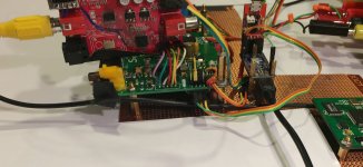
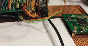
In the meantime, I seem to keep revising my approach as to how to go about setting up for work on master mode I2S. I think I will use one Arduino for both boards, SRC and DAC, since both use different I2S addresses.
Although I said there would be no pin lifting to modify the SRC board, when it came time for me to start working on it I did lift some pins on the microcontroller. Also had to rewire and temporarily disable SPDIF on the DAC board. I needed to get to another signal down in there somewhere.
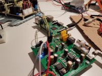
Right now things are pretty much wired up for test, and register programming for the SRC has completed a first pass. Register programming for the DAC is next. A few pictures of the wiring are posted below. It can be seen where 30 AWG wire wrap wire has been attached to the I2S lines for the SRC chip. They go up to a connector where the I2S bus from the Arduino can be plugged in.
The board on the far right is an Arduino Pro Trinket 3.3v with a FTDI card attached to it vertically. The FTDI board allows real time terminal access to the running Arduino program.
In the meantime, I seem to keep revising my approach as to how to go about setting up for work on master mode I2S. I think I will use one Arduino for both boards, SRC and DAC, since both use different I2S addresses.
Although I said there would be no pin lifting to modify the SRC board, when it came time for me to start working on it I did lift some pins on the microcontroller. Also had to rewire and temporarily disable SPDIF on the DAC board. I needed to get to another signal down in there somewhere.
Right now things are pretty much wired up for test, and register programming for the SRC has completed a first pass. Register programming for the DAC is next. A few pictures of the wiring are posted below. It can be seen where 30 AWG wire wrap wire has been attached to the I2S lines for the SRC chip. They go up to a connector where the I2S bus from the Arduino can be plugged in.
The board on the far right is an Arduino Pro Trinket 3.3v with a FTDI card attached to it vertically. The FTDI board allows real time terminal access to the running Arduino program.
Attachments

Regarding 16-bit operation, no problem here with Windows. How is the DAC board connected to the Rasberry Pi3? Using SPDIF, I2S, TOSLINK?
Most likely there is some problem with the interface formatting. Left or right justified, frame size, etc.
Regarding Spotify in particular, the DAC only supports PCM or DSD. There is no MP3 decoder, the computer OS has to do that. Spotify mp3 bitrates are very low, 128kbps, IIRC. The PCM sample rate might only be 22kHz, 11kHz or something like that, which maybe is lower than the DAC supports.
Windows and most OS'es will resample the default sound device audio stream to some common sample rate that can be user configured. They do that so that multiple audio streams can play at once, such as system sounds like mouse clicks, alarms, notifications, etc., playing at the same time while music is playing. Therefore they may send the DAC a standard format it knows how to play.
Rasberry Pi3 OS may not do that, probably not since it takes some computing power to do the SRC in real time even if not all that high quality.
Markw4, thanks for reply. I connected Raspberry pi 3 via I2S directly. I try to find, why is 16 bit unsupported. Unfortunately I have no equipmet for scan I2S. Maybe I try use arduino like signal generator for I2S. Markw4, How is your DAC board connected to the PC? Are you tried play music with setting like 16bit/44100Hz or 16bit/192000Hz? Works it? Maybe is bug only in I2S and spdif is ok?
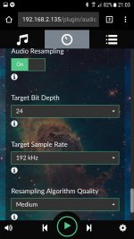
My opinion is, Volumio have decoders for diffrent audio formats (mp3, flac, spotify, ...). But decoded output is send directly to DAC. There is no default resampling like on Windows. If user want, he or she must explitic enable it. Mp3 decoder decode to 24bit? Flac is decoded as is. Spotify is a plugin and volumio don't apply resampling on it. It make me sense from my tests. Resampling off - mp3 OK, 16bit flac FAIL, spotify FAIL. Resampling on - mp3 OK, 16bit flac OK, spotify FAIL.
Attachments
ESS recommends using AD797 opamp in the output stage. The AD797 is similar to the NE5534 with high open loop gain for low noise application. It seems to me that I should leave the NE5532 alone on the Chinese DAC board.For ESS recommended circuits please see the "Maximizing ...performance... " document in the link that follows. Please read carefully and completely. ESS Technology :: Downloads
One thing that is not shown in that document is how to derive the Reference voltage from AVCC. That part is shown in the Evaluation Board Schematic available at the same link.
I was thinking about using the BB OPA627, but not sure anymore from the ESS app note. Any comment?
The Benchmark DAC-3 uses LME49860 opamps. That is a higher voltage version of an LME49720. They run at +-18 volts. Right now I am running my board at about +-17 volts which is within the specs of everything.
The 5534 in there is mostly a problem because it is part a voltage mode output stage with -75dB distortion. If one decides to fix the distortion it requires going to IV output of some kind. If going to that much trouble, may as well use an opamp known to work well based on ESS recommendations, and I would say, Benchmark could be a pretty good recommendation too.
Playing around with swapping opamps in the voltage mode circuit is a gimmick the Chinese DAC makers use to help sell more DACs. It gives various flavors of high distortion with user choice of a little coloration to taste. It's basically junk, but it is cheap to make and it sells. Can't blame them if they understand the market they are catering to. As one can probably tell, I am a strong proponent of going to a good IV output stage. It does sound better, potentially hugely better if other mods are done too.
The problem is the NE5532 is configured as a differential to single ended buffer. The 9038q2m wants an I/V.
You could make a superb NE5532 I/V if you want and get infinitely better performance than the stock board. It's less about the opamp than the configuration.
Edit, seems like Mark beat me to the punch.")
As far as recommended I/V's, look up my username on this thread and you'll see a link to Victor's I/V, or JenH has his schematic, or the ESS provided one. They're generally variations off one another (although Victor's is a clever way to get SE out of one stereo opamp)
You could make a superb NE5532 I/V if you want and get infinitely better performance than the stock board. It's less about the opamp than the configuration.
Edit, seems like Mark beat me to the punch.
As far as recommended I/V's, look up my username on this thread and you'll see a link to Victor's I/V, or JenH has his schematic, or the ESS provided one. They're generally variations off one another (although Victor's is a clever way to get SE out of one stereo opamp)
Last edited:
That I2C analyzer output is pretty hard to read. 0x90 is the write address of the Q2M, and 0x91 is the address for reads. The next bus write after the device address is the register address, and after that another write operation without releasing the bus will overwrite the register contents. To read I2C a bus write is performed to select a register then the device read address is used to read the register contents. There is more too it, fast and slow modes, auto increment register addressing sometimes, etc., but just trying to give a few basics here.
It helps a lot if it is written more like:
Write 0x2B 0x30
write 0xC2 0x00
read 0x00
etc., and where 'write' means address 0x90 was used, and 'read' means address 0x91, then the first byte is the register address, followed by a data byte.
However, even at that a Q2M datasheet is needed to decode. Probably okay to say they use decimal numbering and bits, and don't seem to go for much for hex. You get the idea though.
From looking at boot up bus activity using my own analyzer, my impression is that the code is not entirely rational.
My suggestion, if specific problems with 16-bit I2S, would be to pad out the data with zeros to 24 bits, justified left or right whichever works, or go to SPDIF. Not practical to re-code their firmware.
Also, a potential problem with I2S is that different people have used different naming conventions at times in the past and so to be sure about what is expected it may be necessary to look at timing diagrams in a data sheet.
It may also be helpful to know that some jumper configuration tables for the DAC may be written so that 0=jumper and X=no jumper. Possibly inverted from what one might expect.
Regarding use with Raspberry Pi may I ask if the DAC works when sent SPDIF or TOSLINK from a full-sized computer? Just trying to understand if it ever works at all in any way? If not, the best action might be to contact the seller. They usually wish to avoid bad ratings and will make some effort help to sort out the problem, although language can sometimes be a barrier to effective technical communication, IME.
EDIT: Another question would if the Lock LED on the DAC ever lights up?
Last edited:
It took me a few days. I finally figured out that "I/V" means running the opamp in inverted mode.The problem is the NE5532 is configured as a differential to single ended buffer. The 9038q2m wants an I/V.
You could make a superb NE5532 I/V if you want and get infinitely better performance than the stock board. It's less about the opamp than the configuration.
Edit, seems like Mark beat me to the punch.
As far as recommended I/V's, look up my username on this thread and you'll see a link to Victor's I/V, or JenH has his schematic, or the ESS provided one. They're generally variations off one another (although Victor's is a clever way to get SE out of one stereo opamp)
If I prefer the balanced analogue output, I understand that one leg of the output is in non-inverted mode and the other in inverted mode. Using the same opamp, both legs should have similar characteristics. If I run single ended output, I do not understand how the inverted leg can be better than the non-inverted leg.
If we run the opamp in unity gain, the noise performance should not deteriorate. The +-15 volts supply should give it plenty of headroom.
I may misunderstand the meaning of "I/V" or miss other critical aspect. Please, help.
I/V does not mean inverted, although that is a byproduct. ESS says the DAC outputs can be run into a high-ish impedance load, they call that voltage mode. Or the outputs can be run into a virtual short to ground (AC-wise), which they call current mode. I/V stands for 'current to voltage' conversion.
In reality with I/V the outputs aren't held at virtual ground by the I/V opamps, rather they are held at an offset from ground called the 'reference' voltage. The reference voltage is exactly 1/2 of AVCC, the DAC chip analog output power supply voltage.
In can help greatly if you ask questions about anything that is not clear in some of these technical discussions. People are willing and happy to help.
Anyway, ESS says distortion is greater when the DAC outputs are operated in voltage mode and best when operated in current mode. They aren't kidding. The circuit that comes with the DAC uses what amounts to voltage mode. That's bad.
If using current mode there are two DAC outputs for each channel, one inverted and one non-inverted. Both are converted from currents by going into two separate I/V opamp stages (one for each output), then used that way as differential outputs, or they may be combined into one single-ended output per channel using another opamp as a differential summing circuit.
As DPH said, victor figured out a clever way to do the whole operation using only one dual-opamp per channel.
Again, if anything not clear please say so.
Last edited:
Thank you. Now it makes lots of sense to me. It would be nice if someone create a plug-in daughter card for this purpose.I/V does not mean inverted, although that is a byproduct. ESS says the DAC outputs can be run into a high-ish impedance load, they call that voltage mode. Or the outputs can be run into a virtual short to ground (AC-wise), which they call current mode. I/V stands for 'current to voltage' conversion.
In reality with I/V the outputs aren't held at virtual ground by the I/V opamps, rather they are held at an offset from ground called the 'reference' voltage. The reference voltage is exactly 1/2 of AVCC, the DAC chip analog output power supply voltage.
In can help greatly if you ask questions about anything that is not clear in some of these technical discussions. People are willing and happy to help.
Anyway, ESS says distortion is greater when the DAC outputs are operated in voltage mode and best when operated in current mode. They aren't kidding. The circuit that comes with the DAC uses what amounts to voltage mode. That's bad.
If using current mode there are two DAC outputs for each channel, one inverted and one non-inverted. Both are converted from currents by going into two separate I/V opamp stages (one for each output), then used that way as differential outputs, or they may be combined into one single-ended output per channel using another opamp as a differential summing circuit.
As DPH said, victor figured out a clever way to do the whole operation using only one dual-opamp per channel.
Again, if anything not clear please say so.
What do you think of the Zen I-V converter by Nelson Pass? Pass always emphasizes simplicity.
Any Chinese ES9038Q2M board with the I-V designed in? Do the Topping D50, SMSL M8A or Pro-Ject 2S use I-V in their output?
Last edited:
What do you think of the Zen I-V converter by Nelson Pass? Pass always emphasizes simplicity.
Any Chinese ES9038Q2M board with the I-V designed in? Do the Topping D50, SMSL M8A or Pro-Ject 2S use I-V in their output?
Please recall the the IV stages are not actually virtual grounds and you would need a total of four of them, two for each channel. Building four Zen's and modifying them to work at a reference voltage rather than ground might be a lot to take on. Especially when you consider the following:
I/V output stages are not the only issue. Not by a long shot. According to ESS, AVCC should have a super-regulated power supply. It has zero PSRR and is critical to sound quality. So, that needs fixing. From that, reference voltages need be derived.
Power supply regulation on the board is poor, with digital and analog circuitry on the same power rails. Bad.
The clock is not a low-jitter type. Bad.
The reconstruction filters built into the DAC chip have audible artifacts in the audio band. Not great.
For perhaps more than one reason, some of which may not be fully understood, these DACs seem to sound better with upsampled inputs. For example, Benchmark and the latest 5th-generation Crane Song DACs use upsampling. Crane Song has an extremely low-jitter clock and say it is is a big deal. I know a guy who sells gear to recording and mastering facilities. He is well-known in the industry but keeps a low profile for reasons I will set aside for the moment. He sells a lot of Benchmark and some mastering facilities are buying some Crane Song units unlistened-to based on previous experience with earlier products that have become mainstays. Both Benchmark and Crane Song are using upsampling and custom reconstruction filters to address the audibility issues. Don't know about other high-end manufacturers at this point, but no doubt they are watching. What I can say is this DAC sounds better with upsampling and use of a slow transition minimum phase reconstruction filter. There is a lot to do to bring these DACs up to a level of quality that makes full use of what the Q2M chip is capable of. It can cost $200 or more by the time one is done to make this DAC into a serious very detailed accurate and great sounding DAC. That is cheap for what you get, but it is plenty complicated without trying to get rid of the opamps. If used wisely they are fine. That's not the problem, not even something to think about until you have done all the other stuff that matters more.
In addition to all the foregoing I am working on testing one remaining mod that is reputed to be a big deal. Probably in a few days I will have more to say on that.
Last edited:
I am thinking given the simplicity of the board, it requires a lot mods to start making it decent. Just look at the list you've just outlined.
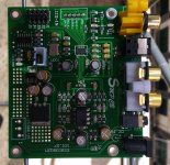
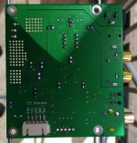
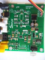
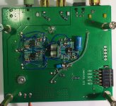
Is the following a better starting point? Seems like a lot less butchering involved to match the ESS recommendations. As you've outlined the grounding on the board looks to be a mess and this is what I am running into as I think how I am going to add an IV circuit to the 38q2m that makes sense. My addition needs to be outboard. I need to bring AVCC in for each channel do I return the ground back to the single q2m board or is it better to take back to a central point like a star ground. Same thing is happening as I look at the 3.3V. My ground returns are shared by analog as well as digital. I can't imagine that is good.
Is the following a better starting point? Seems like a lot less butchering involved to match the ESS recommendations. As you've outlined the grounding on the board looks to be a mess and this is what I am running into as I think how I am going to add an IV circuit to the 38q2m that makes sense. My addition needs to be outboard. I need to bring AVCC in for each channel do I return the ground back to the single q2m board or is it better to take back to a central point like a star ground. Same thing is happening as I look at the 3.3V. My ground returns are shared by analog as well as digital. I can't imagine that is good.
Attachments
Last edited:
Is the following a better starting point?
Not really, IMHO. It has a lot of problems too and will probably end up costing even more to make right. Cheap, low-cost circuitry, and cheap parts except for maybe the name-brand chip. Those guys are getting their costs down as low a possible because they operate in a very cost-sensitive market. Sometimes buyers will chose one seller over another based on a 1-cent price difference. The board you reference is made as cheaply as possible and still make people think it is worth more and a good deal. Maybe it is a good deal, in fact, but not high-quality, and not easily made into high quality.
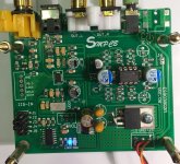
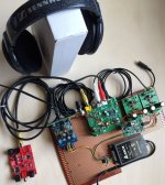
Regarding how to do it, I have posted photos of one way a few times. Don't remember what the posts were. Guess I can do it again. Click on the little white X in the lower left corner to blow up to full size or download and view in full size on a PC.
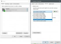
I also added a picture showing how to set the output sample rate for Windows from the sound settings in the control panel. Unfortunately, unless you have ASIO drivers for a sound card that is not the default sound device card, Windows will resample your audio to whatever that setting is and do a poor job of it. If you want to hear it unaltered you will need to reset it to match the sample rate of whatever file you are trying to play. When testing DAC operation, setting it correctly is mandatory or the exercise is probably a waste of time and even worse misleading. Macs do this type of thing too, maybe Linux.
Also, BTW, the power supply shown in the one photo is gone, as is one of the headphone amp options. The headphone amp shown is a modified $32 ebay special and pretty good. You need something you know is good enough to hear and judge DAC sound quality.
The other board is a TI SRC4392 upsampler board available from China for about $60 and worth it. Doesn't need modding to do what it is intended to do but may end up getting modded for this last bit of testing I am doing.
Attachments
Last edited:
I am thinking given the simplicity of the board, it requires a lot mods to start making it decent. Just look at the list you've just outlined.
Is the following a better starting point? Seems like a lot less butchering involved to match the ESS recommendations. As you've outlined the grounding on the board looks to be a mess and this is what I am running into as I think how I am going to add an IV circuit to the 38q2m that makes sense. My addition needs to be outboard. I need to bring AVCC in for each channel do I return the ground back to the single q2m board or is it better to take back to a central point like a star ground. Same thing is happening as I look at the 3.3V. My ground returns are shared by analog as well as digital. I can't imagine that is good.
Link?
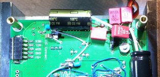
Hi terry22, I wrote up the clock replacement but finding old posts can be challenging sometimes. Temporarily removed the volume pot header and then used Chip Quik solder to remove the old clock. The new clock was slightly bigger, but not by much. All I had to do on that was use an X-acto knife to trim away a bit of ground plane near the solder pads to leave a little more clearance. If you look at my photos of the board you can see how the clearance around the pads is bigger as compared to the decoupling caps nearby. Originally they were all the same. If you can't find a photo I could repost that one.
EDIT: Later I went back and put the clock on its own dedicated 3.3v regulator, mostly as an experiment. By then the power issues had been mostly fixed. The clock is HF analog and not really so much part of the digital circuitry, that was the rationale anyway. It was easy to do and I think it may have helped a small amount, but I can't say it was dramatic.
Hi Mark,
I saw that there is many models of crystek 575, but I guess it is the 100mhz one. is that right?
CCHD-575-50-100.000 Crystek Corporation | Mouser France
You wrote about power issues,
do you think the clock replacement will work and still be an improvement without the dedicated regulator as I don't know if I can do it?
Thank you for your help
- Home
- Source & Line
- Digital Line Level
- ES9038Q2M Board