I'm not that great with technical stuff, I'm more of an assembler and have very little rudimentary engineering knowledge so I would like someone to go over my designs so I can avoid noise and crosstalk. I've done some research myself but would like some feedback from the diyaudio community.
Mainly read from this source: http://www.ti.com/lit/an/szza009/szza009.pdf
PCB Design Guidelines for reduced EMI by Texas Instruments.
But also here: Tips on how to properly design/layout a Printed Circuit Board (PCB)
Tips on how to properly design/layout a Printed Circuit Board (PCB)
Reason why I'm using expresspcb is because I find it easier to use than Kicad or Eagle and it supports metric. You'll need the software to view the file. ExpressPCB -
And with expresspcb I can whip up plug-in prototypes if I stick to using only single sided boards that I can make at home. Its not like I need rocket-science software for a TDA DAC anyway.
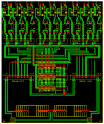
I've designed a more universal mainboard for all DACs so I can sample what is out there without having to rebuild a new chassis over and over for each new DAC, with this I can just punch out some small plug-in boards and try a design change or even try a new DAC IC. It uses 40 pin IDC sockets to connect whatever boards I would like to use into the main motherboard. This is so I can easily plug in a TDA1543 dac into the same motherboard which is setup for use with a TDA1541 and other more modern DACs later down the track.
I've settled on a 7.5 inch wide x 9 inch high main motherboard size, I feel that this size will easily fit into a shallow 2U or 3U chassis with room to spare on the sides and back and front. The plug-in boards can be 2.5 inches or 6.35cm in height, this restriction is because I'm using a 2U chassis. higher boards can be used if I change to using a 3U chassis.
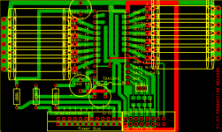
PSUs are plentiful, 8x positive rail voltages and 4x negative rail voltages for the Receiver/Reclock + Oversampling/DAC. In addition to this there are 4x positive rail voltages and 2x negative rail voltages for the preamps. Each 40 pin IDC socket connector for the PSUs can support a total of 6x rails, 4x positive, 2 negative. I intend upon using 3 pin LM317/337 or 78xx regulators which can easily be swapped out for shunt types. if I was using tube-based preamps I would need to turn the last PSU board into low voltage (for filament) and high voltage rails (for B+).
The main idea behind this is so that if I want to change or alter a DAC pcb's layout or design I can simply design a much easier smaller board which can then be plugged into the main motherboard. Same goes for all of the boards, such as the receiver board, reclock/oversampling board, and preamp and PSU boards.
Here is what I have come up with so far, I've left the filter capacitors and diode rectifiers on the mainboard and just used 40 pin IDC sockets for plug-in volt regs. I have made enough room for one Receiver board port, one Reclock/Oversampling board and one DAC board. I have also left enough room on the PCB for two tube preamp boards on either side of the DAC board using 9 pin mini tube sockets.
I have placed areas on the board for two very large axial coupling capacitors. These are for botique types but can also be used for more generic stuff such as the K73-16B 63v 22uF which do fit with room to spare on a printout fitting test.
Inputs are on the receiver board and I'll be making them RP-SMA.
Anyway I would just be happy if someone could check my work first before I send off for a first run.
Mainly read from this source: http://www.ti.com/lit/an/szza009/szza009.pdf
PCB Design Guidelines for reduced EMI by Texas Instruments.
But also here: Tips on how to properly design/layout a Printed Circuit Board (PCB)
Tips on how to properly design/layout a Printed Circuit Board (PCB)
Reason why I'm using expresspcb is because I find it easier to use than Kicad or Eagle and it supports metric. You'll need the software to view the file. ExpressPCB -
And with expresspcb I can whip up plug-in prototypes if I stick to using only single sided boards that I can make at home. Its not like I need rocket-science software for a TDA DAC anyway.
I've designed a more universal mainboard for all DACs so I can sample what is out there without having to rebuild a new chassis over and over for each new DAC, with this I can just punch out some small plug-in boards and try a design change or even try a new DAC IC. It uses 40 pin IDC sockets to connect whatever boards I would like to use into the main motherboard. This is so I can easily plug in a TDA1543 dac into the same motherboard which is setup for use with a TDA1541 and other more modern DACs later down the track.
I've settled on a 7.5 inch wide x 9 inch high main motherboard size, I feel that this size will easily fit into a shallow 2U or 3U chassis with room to spare on the sides and back and front. The plug-in boards can be 2.5 inches or 6.35cm in height, this restriction is because I'm using a 2U chassis. higher boards can be used if I change to using a 3U chassis.
PSUs are plentiful, 8x positive rail voltages and 4x negative rail voltages for the Receiver/Reclock + Oversampling/DAC. In addition to this there are 4x positive rail voltages and 2x negative rail voltages for the preamps. Each 40 pin IDC socket connector for the PSUs can support a total of 6x rails, 4x positive, 2 negative. I intend upon using 3 pin LM317/337 or 78xx regulators which can easily be swapped out for shunt types. if I was using tube-based preamps I would need to turn the last PSU board into low voltage (for filament) and high voltage rails (for B+).
The main idea behind this is so that if I want to change or alter a DAC pcb's layout or design I can simply design a much easier smaller board which can then be plugged into the main motherboard. Same goes for all of the boards, such as the receiver board, reclock/oversampling board, and preamp and PSU boards.
Here is what I have come up with so far, I've left the filter capacitors and diode rectifiers on the mainboard and just used 40 pin IDC sockets for plug-in volt regs. I have made enough room for one Receiver board port, one Reclock/Oversampling board and one DAC board. I have also left enough room on the PCB for two tube preamp boards on either side of the DAC board using 9 pin mini tube sockets.
I have placed areas on the board for two very large axial coupling capacitors. These are for botique types but can also be used for more generic stuff such as the K73-16B 63v 22uF which do fit with room to spare on a printout fitting test.
Inputs are on the receiver board and I'll be making them RP-SMA.
Anyway I would just be happy if someone could check my work first before I send off for a first run.
Attachments
Fixed a few fatal problems.
Changes:
1) Reduced the pin count of the data bus from 16 pins to 8, I figured this should be plenty enough and I want to keep the option of using single sided boards for plug-ins.
2) Swapped the power and gnd sides of each 40 pin connector to better reflect pcb orientation when using 40 pin 90 degree female connectors. PCB orientation is now top towards coupling capacitors and the whole row of the bottom of each connector is now an earth.
Attachments
Updated all four boards. Thickened traces in some areas and thinned them in others.
I haven't completely double checked the wiring as of yet but it seems to be all in the correct places.
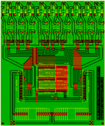
The reason why I'm starting with this arrangement of chips is because I want to get something that works first and foremost then create additional plug in boards which will then upgrade performance such as a new receiver chip. That is the good thing about this plug-in arrangement because I can easily remove and replace a receiver or reclock circuit with a better newer one just by designing and plugging a new board in.
I didn't bother with a NOS switch on the SAA7220 board because I ran out of space. Plus I figured I can whip up a small board which will replace the SAA7220 board entirely and replace it with just traces going to the DAC stage. Not having those chips on the data bus means I can also create a much better 74HC4040 board with just a reclocking stage.
I've also left the top copper traces as short as possible so I can simply use wires to jumper across the bottom copper traces and still remain faithful to the single sided homebrew board compatibility rule. Though the main motherboard breaks that rule and I would suggest to anyone who is going to do this project to simply buy the main motherboard and produce the other boards at home.
What I might do actually in version 1.3 of the main mobo is move the preamps back to the same height as the SAA7220/reclocking board so then I can have a bit more room to make the main DAC board wider so I can use more botique capacitors as decoupling capacitors (Such as the K40Y-9 0.1uF PIO caps), but I haven't decided yet. I haven't decided yet mainly because if I'm going to be using a tube preamp stage the tubes might conflict with the size of the DAC board which wouldn't be any good and moving the preamp boards further down might conflict with the large coupling capacitors on the main motherboard.
I haven't completely double checked the wiring as of yet but it seems to be all in the correct places.
The reason why I'm starting with this arrangement of chips is because I want to get something that works first and foremost then create additional plug in boards which will then upgrade performance such as a new receiver chip. That is the good thing about this plug-in arrangement because I can easily remove and replace a receiver or reclock circuit with a better newer one just by designing and plugging a new board in.
I didn't bother with a NOS switch on the SAA7220 board because I ran out of space. Plus I figured I can whip up a small board which will replace the SAA7220 board entirely and replace it with just traces going to the DAC stage. Not having those chips on the data bus means I can also create a much better 74HC4040 board with just a reclocking stage.
I've also left the top copper traces as short as possible so I can simply use wires to jumper across the bottom copper traces and still remain faithful to the single sided homebrew board compatibility rule. Though the main motherboard breaks that rule and I would suggest to anyone who is going to do this project to simply buy the main motherboard and produce the other boards at home.
What I might do actually in version 1.3 of the main mobo is move the preamps back to the same height as the SAA7220/reclocking board so then I can have a bit more room to make the main DAC board wider so I can use more botique capacitors as decoupling capacitors (Such as the K40Y-9 0.1uF PIO caps), but I haven't decided yet. I haven't decided yet mainly because if I'm going to be using a tube preamp stage the tubes might conflict with the size of the DAC board which wouldn't be any good and moving the preamp boards further down might conflict with the large coupling capacitors on the main motherboard.
Attachments
Last edited:
PSU pcb is completed for PSUs 1 and 2. This design is meant to take tentlabs shunt regulators but could also use 78xx/79xx regs in a pinch if you can't/don't want to buy the expensive shunt regulators or just want to get something working to try it out on. 78xx type regs aren't the best out there in terms of noise performance.
Attachments
V1.4 for TDA1541 PCB and main motherboard.
1) Moved the two preamp boards back to the same height as the SAA7220 pcb.
2) Changed the TDA1541 pcb to make it 4 inches wide to accommodate unusual sized decoupling capacitors but I've also left in the traces for SMD components so I can try both.
3) Changed the main motherboard to flip which side the voltages go for the left side preamp board. This is so I can have the vacuum tube on the left side of the pcb for the left preamp and right side of the pcb for the right preamp.
To use K40 capacitors you'll need to attach one to the top of the PCB and one to the rear.
Attachments
Version 1.5 of the main motherboard is designed for a homemade production process.
Every "top layer copper" is therefore replaced with a wire trace which needs to be routed as displayed on the pcb design. Only well insulated wire with a high tensile strength will suffice. A lot of hot glue will also probably be needed if you or I am going to use stranded wire. However using bendable single strand copper wire will allow me to route the cabling around each pin.
I will need to attempt to do a print transfer before I can officially say that it will work but I think it is ready for a first attempt.
I've also reduced the length of most of the power supply traces and rerouted them to give the board an overall cleaner look.
Attachments
The TDA1541 DAC plug-in board has been released for evaluation by diyaudio. Version is v1.51 and this PCB is marked as a production release, so its close to being set in stone.
All components are deliberately left undefined. This is an experimenters DAC and I'm not an engineer so I cannot tell you what components to use. Its all up to you. But a bit of digging around on the forum will show some suggestions on what to use and where and why.
I've replaced the old main filtering capacitors with 10mm diameter ones and I've added bottom copper layer traces for 1206 SMD capacitors on the VDD of each input rail.
Would love some input on the design of it however. The DGND and AGND connection is made at pin 14.
If you are going to be making homemade PCBs then all top copper layer traces are jumper wires. This PCB is designed to be manufactured in a single bottom copper layer OR converted into gerber and prefabbed as a 2 layer board.
Once all of the plug-in boards are completed I'll bunch them all up into one file and covert that single file into gerber. Assuming expresspcb will allow me to do that.
Attachments
Last edited:
Main mobo has reached v1.51 production release. Just had to fix a few things with grounding. This mobo would work both as a homemade or prefabbed. As a single layer board you will need to jumper the power and data lines with wire but you will lose the shielding on the data lines.
Attachments
- Status
- This old topic is closed. If you want to reopen this topic, contact a moderator using the "Report Post" button.
- Home
- Source & Line
- Digital Line Level
- A DAC motherboard to hold 40 pin IDC sockets for plug-in homemade PCBs