Thanks for your answers.
Long story short, when I want decent information, I’ll probably have to build the Dac to get useful answers.
But before that I will give it a last try with LTSpice with much lower frequencies with parametrized rise, fall and delay times for the various components.
Maybe that could still reveal something.
Could you still respond to my questions how the two 3n3 caps at the summation points of the FirDac where calculated and wether a 4 stage FirDac could bring any benefit ?
Hans
When you exaggerate the difference between rise and fall times such that it becomes a substantial part of half a clock period, simulating their impact should become much easier. You only need very accurate simulations when you first do your utmost to minimize these differences and then want to check what impact the remainder has.
The longer the FIRDAC the better. I also use four stages, by the way.
Digging up my filter calculations will take some time, especially when they are in the attic, as I have no access to it until Thursday.
The longer the FIRDAC the better. I also use four stages, by the way.
Digging up my filter calculations will take some time, especially when they are in the attic, as I have no access to it until Thursday.
Last edited:
The only information I could retrieve without the attic is that it's a sixth-order Gaussian-to-6 dB filter with an extra negative real pole. I've tweaked that negative real pole to get the roll-off over the audio band to match with the filter of the valve DAC, so the digital precorrection should work for both. The negative real pole gives some extra passive filtering before reaching the first op-amp, to prevent slewing-induced distortion.
Theoretically, including resistor value rounding, the poles are
-1.248 Mrad/s and (-273691 +/- 171759 j) rad/s for the first stage
(-233904 +/- 500150 j) rad/s for the second stage
(-110101 +/- 752736 j) rad/s for the third stage
The ideal values for Gaussian-to-6 dB are
(-271665 +/- 171562.5 j) rad/s
(-233613.5 +/- 499550 j) rad/s
(-110183.5 +/- 753361.5 j) rad/s
How on Earth this leads to 3.3 nF is something I can't answer without looking in the attic.
Marcel,
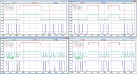
Here's the outcome of my simulation
I have used a reduced 2.5Mhz clock to get a better view on what's happening.
Of the four graphs below in the first image, the left side produces 0011000 and the right side 0010100.
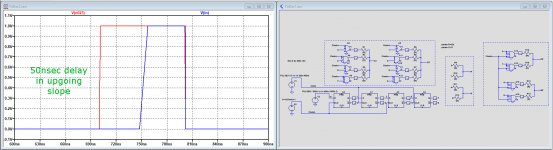
In the upper half, the up- and down-going flanks are untouched with a 50% duty cycle 2.5Mhz signal, but in the lower half all upgoing flanks are delayed by 50nsec, see second image.
This already leads to rather terrible looking signals, and as mentioned before, when up- and down-going flanks are not happening at the same time, one will get spikes with the topology you used, see the teal lines.
These spikes do not happen when taking out the NOR circuits and to get a true RTZ version in Blue with half cycles.
However both versions suffer to the same amount in their average value between 1010 and 1100.
But the big surprise is that in all cases the most simple version, with resistors only connected to the FFs, keep it's average value constant at 333.33mV in all situations as shown in the 4 inserts.
This can IMO only be explained because of the 2 segment FirDac that nihilates the timing differences.
See the boxed part in the middle of image two, ending in the signals P and N.
Also note that this signal was divided by two to make it comparable in level to the other two signals, but in fact it is 6dB larger.
Looking forward to see your comments.
Hans
.
Here's the outcome of my simulation
I have used a reduced 2.5Mhz clock to get a better view on what's happening.
Of the four graphs below in the first image, the left side produces 0011000 and the right side 0010100.
In the upper half, the up- and down-going flanks are untouched with a 50% duty cycle 2.5Mhz signal, but in the lower half all upgoing flanks are delayed by 50nsec, see second image.
This already leads to rather terrible looking signals, and as mentioned before, when up- and down-going flanks are not happening at the same time, one will get spikes with the topology you used, see the teal lines.
These spikes do not happen when taking out the NOR circuits and to get a true RTZ version in Blue with half cycles.
However both versions suffer to the same amount in their average value between 1010 and 1100.
But the big surprise is that in all cases the most simple version, with resistors only connected to the FFs, keep it's average value constant at 333.33mV in all situations as shown in the 4 inserts.
This can IMO only be explained because of the 2 segment FirDac that nihilates the timing differences.
See the boxed part in the middle of image two, ending in the signals P and N.
Also note that this signal was divided by two to make it comparable in level to the other two signals, but in fact it is 6dB larger.
Looking forward to see your comments.
Hans
.
Attachments
What are the average voltages? I only see the values for the flip-flops.
Regarding the flip-flops, in a balanced structure, when the rise and fall time difference for the positive and negative outputs is the same, which it never exactly is, they compensate each other. I would expect that when you look at only P or only N, you get the biggest error of the whole circuit.
Regarding the flip-flops, in a balanced structure, when the rise and fall time difference for the positive and negative outputs is the same, which it never exactly is, they compensate each other. I would expect that when you look at only P or only N, you get the biggest error of the whole circuit.
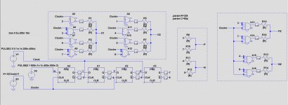
What you see are the differential voltages between resp. O1&O2, P&N and PZ&NZ, please see the encircled boxes in the above circuit diagram for what they are doing.
Also look at the text in the header of the LTSpice images, here you can see exactly what is shown, including the offset that was given not to let the images fall on top of each other.
And no voltages from FlipFlops are visible in the images as you may have thought.
The logic modules from LTSpice are switching between 0Volt and 1Volt with a tripping point at 0.5Volt.
The rise and fall times for the FlipFlops on both outputs are not the same, only the rise time is affected for both outputs with the little square subcircuit that was added to all digital outputs as you can find in the circuit diagram.
I haven’t looked in detail at the individual P or N signal, but I will to cover that part tonight.
Hans
In the upper left corner of each of the four simulation plots on the left, I see that V(P,N)/2 is on average 333.33 mV. The schematic shows that V(P) is the average of the voltages at nodes 3 and 7, which are delayed flip-flop outputs, and V(N) is the average of the voltages at nodes 4 and 8, also delayed flip-flop outputs.
In a balanced structure, when the rising delay is the same for the positive and the negative output, the rise time is the same for the positive and the negative output, the falling delay is the same for the positive and the negative output and the fall time is the same for the positive and the negative output, the error due to unequal delays drops out of the equation. That's because there is always one side going up and one side going down on each and every transition.
In a balanced structure, when the rising delay is the same for the positive and the negative output, the rise time is the same for the positive and the negative output, the falling delay is the same for the positive and the negative output and the fall time is the same for the positive and the negative output, the error due to unequal delays drops out of the equation. That's because there is always one side going up and one side going down on each and every transition.
Last edited:
Regarding the spikes, the narrow spikes in the green signal should be easier to filter off with a passive RC section than the much wider troughs in the blue signal, so why do you regard them as a problem?
At this frequency spikes with a BW in the 100Mhz range aren’t that easy to filter.
That’s what concerned me.
The wide RTZ throughs in the blue signal are simply the 27Mhz clock that’s part of the signal in all 3 investigated versions when the SDM is running with music.
So this 27Mhz has to be filtered anyhow, but may be less bening as the Spikes in the HF range.
But at the moment I think that both the blue and the teal signal are inferior to the red signal.
Hans
In the upper left corner of each of the four simulation plots on the left, I see that V(P,N)/2 is on average 333.33 mV. The schematic shows that V(P) is the average of the voltages at nodes 3 and 7, which are delayed flip-flop outputs, and V(N) is the average of the voltages at nodes 4 and 8, also delayed flip-flop outputs.
Delayed only for the rise time, not for the fall time.
Hans
I just reread post #45 a bit more carefully and apparently it was your intention to print only the averages of those voltages. In any case, why they are equal is explained in post #49.
For the other outputs, for some reason there is a spike missing in the bottom right pictures compared to bottom left. I don't know why. Is it some sort of initial transient or do you see the same when the pattern is periodically repeated?
For the other outputs, for some reason there is a spike missing in the bottom right pictures compared to bottom left. I don't know why. Is it some sort of initial transient or do you see the same when the pattern is periodically repeated?
Yes, I printed the average of the processed waveforms, because 0101 and 1100 should give the same average, independent from rise or fall time.
So far only the red line passed this test.
But what I did was just some first attempt with the extended rise times.
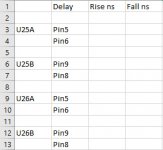
What I propose however to get the same mutual view on things is that if possible you write above each little subcircuit square what delay in either Rise or Fall time is appropriate to your opinion for this test and return the jpeg to me.
I then set all rise or fall delays individually and do the test again.
Hans
.
P.S. I don't see a missing spike ?
So far only the red line passed this test.
But what I did was just some first attempt with the extended rise times.
What I propose however to get the same mutual view on things is that if possible you write above each little subcircuit square what delay in either Rise or Fall time is appropriate to your opinion for this test and return the jpeg to me.
I then set all rise or fall delays individually and do the test again.
Hans
.
P.S. I don't see a missing spike ?
Attachments
Last edited:
P.S. I don't see a missing spike ?
When I count the spikes, I see a difference of 1 spike between the bottom left and right pictures. Don't you?
It's actually intended, because the curve with two wide pulses has one spike less than the curve with one wide pulse, so the number of rising and falling edges is the same. Duh...
Last edited:
Yes, I printed the average of the processed waveforms, because 0101 and 1100 should give the same average, independent from rise or fall time.
So far only the red line passed this test.
But what I did was just some first attempt with the extended rise times.
What I propose however to get the same mutual view on things is that if possible you write above each little subcircuit square what delay in either Rise or Fall time is appropriate to your opinion for this test and return the jpeg to me.
I then set all rise or fall delays individually and do the test again.
Hans
.
P.S. I don't see a missing spike ?
As you already see unintended behaviour with your present simulation testbench, I propose to first find out where it's coming from before adding further imperfections. As an attempt to narrow in on the issue, you could kick out the last two flip-flops, the gates driven by them and the whole negative side to see what that does. Please print the averages that are pattern-dependent, maybe that gives a hunch why they are pattern-dependent.
Adding more imperfections is for later, after debugging the issue you found.
My circuit only works well when the delay of the flip-flops is of the order of the gate delay or more. That is, a low-to-high transition at a NOR gate input is supposed to make the NOR gate insensitive to what happens at the other input before the flip-flop output starts switching. In fact that's why JohnW prefers circuits with more clock phases, to get a more well-defined delay.
Does adding a delay in both directions (unequal, of course) to the flip-flop outputs change anything in your simulation?
Did you switch off the damn waveform compression? .opt plotwinsize=0 is the way to let it remember that you turned it off, otherwise it turns it on and produces complete crap again whenever you start a new LTSpice session.
Last edited:
Wow, I ALWAYS turn both on, but this seems an exception to the rule where I forgot it. 
You suggest to apply as a next step different delays to the FFs, I fully agree that it's more realistic.
Please advise what delay values to use, that will prevent miscommunication and wasted time for both of us.
Momentarily in the Spice model running 10 times slower, I've used 50 nsec delay in risetime and nothing in falltime, in the real version this would be something like 5 nsec.
In the table below, added as a zipped Excel file, you can enter all kind of delays in rise and fall times and return the data to me, just a few minutes work, is that O.K. ?
Hans
.
Attachments
- Home
- Source & Line
- Digital Line Level
- 74AHC02 and 74AHC08 DAC with 97 dB(A) dynamic range