Even 64 is adequate to eliminate quantization noise by simple 12dB/oct RC filter.
I intended if you use 5bit DAC for DSM, simple 12dB/oct is adequate for 64OSR. But I guess you use 1bit of 512OSR which means the out of band noise increases almost from 300kHz because the latest 1bit of 64OSR is from 40kHz. If so, you can have a decent signal up to even 85kHz.
I am also a little bit surprised the 3rd stage(U7B) has the gain against the out of band noise. Even if it is measured from the peak-peak signal, The output of LPF is usually smaller than the input. Two layers PCB can't have stable ground potential and tends to result in faulty measurement. But your PCB has four layers including a plane ground. I wonder what makes such phenomena.
Attached is a zip with updated Verilog files and UCF file. The new files add an I2S input that can be switched to raw DSD64 and raw DSD128 modes, the gain for DSD has been updated such that there is no volume difference between Scarlet Book compliant DSD and PCM anymore (non-Scarlet Book DSD can still be played in the medium and soft modes) and the interfacing to the FIFOs has been improved. I think I also fixed the switch-on thump. See https://linearaudio.net/sites/linearaudio.net/files/additionaldatavalveDACversion2p1.zip for a version with MCS file.
Attachments
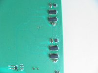
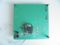
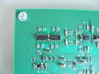
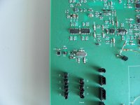
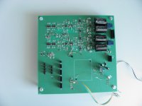
I have no pictures, but I could take some if you want. It's just a four-layer PCB with a bunch of SMD components on both sides.
Building it cost me about 500 euro, almost half of that is for the FPGA module. A couple of months ago the FPGA modules were suddenly some 100 euro cheaper, but apparently that was because Trenz wanted to get rid of old stock after a hardware revision, they are back at their old price now.
Since you are a DSD fan, it is only fair to warn you that the DAC handles DSD by decimating it to 201.6 kHz PCM, passing it through an asynchronous sample rate converter, interpolating it and converting it back into a sigma-delta modulate.
A DSD-only version with only a raw DSD interface and no decimation, just like the Signalyst DSC1, would be much cheaper because it wouldn't need the FPGA module, nor the SRC4392 ASRC chip, nor the DIX4192 S/PDIF interface.
These are the pictures. A DSD-only version with raw DSD interface could be about half the size, see https://www.diyaudio.com/forums/digital-line-level/273474-dac-dac-224.html#post5830769 post 2237 for a schematic with incorrect filter component values.
Attachments
For what it's worth, it sounds quite neutral to me, but I haven't listened to it much and I certainly haven't done any controlled listening tests. I've mainly used it for experiments and for testing new configuration files for my valve DAC's FPGA without needing potentially lethal voltages.
For completeness: some time ago I've made a version 3 of the valve DAC configuration file that runs on a somewhat cheaper FPGA module, see https://www.diyaudio.com/forums/dig...linear-audio-volume-13-a-152.html#post6569767 and https://www.diyaudio.com/forums/dig...linear-audio-volume-13-a-153.html#post6570538 . It also works with this solid-state DAC.
Hi Marcel,
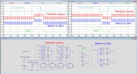
1) Because I didn't fully understand the FirDac in your 74AHC02 design, I simulated this part.
Looking at the image below, you see the input signal on top.
In the graph at the left a positive pulse and at the right a reversed pulse is used as input signal.
Second graph below in Red shows what the design with XORs is doing.
Third in Blue, shows a Return to Zero that is the one it should be IMO.
Fourth graph at the bottom shows the outcome when not applying return to zero.
Notice that I had to divide all signals by 2 to give them the same amplitude as the 74AHC02 design with XORs, so in fact 6 dB is gained here. No idea what effect this has on the noise floor and/or distortion.
2) when following the design that I made, two FlipFlops and 4 XORs become obsolete, so a 4 segment FirDac could easily be made with these freed FFs and And gates replacing the XORs.
If so, would it make sense to equip the 4 segments with some weighting factors to assist the later filtering process ?
3) The 3n3 caps as part of your FirDac, how was this value calculated ?
Hans
Attachments
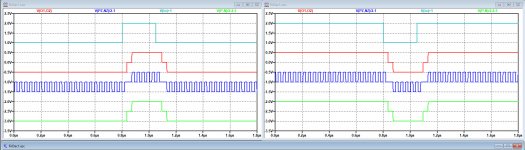
It's a FIRDAC with half cycle delays. If it works as intended, each individual gate switches to zero, thereby eliminating the effect of unequal rising and falling delays. The output of the entire FIRDAC is a sum of RTZ waveforms shifted by multiples of half a cycle and does not switch to zero: in every half cycle, two gate outputs are switched to zero while the other two output data.
O.k. So the sim is showing the correct signal this time.
I’ll take some time to understand why unequal rise and fall time in the version without gates is worse.
With those half cycles, you have to complement the second half, masking the rise or fall time of the first half. But this complement also has a rise or fall time at the end of the full cycle.
Why is this edge then superior to the original signal from the FlipFlop.
Isn’t just something taken away and the complemented with a similar signal ?
Hans
For a start, look at one single gate:
When the gate reproduces a 001100 bit pattern, as it is switched back to zero every time, you actually get 000001010000, so two rising and two falling edges, two ones and 10 zeros.
When the gate reproduces a 010100 bit pattern, as it is switched back to zero every time, you actually get 000100010000, so two rising and two falling edges, two ones and 10 zeros. That is, the average is exactly the same as for the other pattern, as it should be.
The whole FIRDAC just produces the average of four signals like this, so it also has an average output signal level that's independent of whether the bit pattern is 010100 or 001100.
The flip-flop has only one rising and one falling edge for 001100, so it has a different average output level than for 010100.
Whether this matters depends on how you generate the one-bit signal. When you have an embedded pulse width modulator, don't randomly rotate its pattern and exclude the code where all bits are one, then you already have a return to zero function built into the modulator. I do randomly rotate the pattern to get rid of PWM modulator distortion and I don't exclude any patterns, so it matters with my modulator algorithms.
Last edited:
Marcel,
The two half cycle signals, being added to a obtain full cycles, are switching most of the time in opposite directions.
When having the slightest differences in the switching on/off slope steepness as well as in propagation delay, this will produce HF noise on the summed line.
And inevitably, there still are points left where only one half cycle is switching up or down while the other half is constant for two consecutive half cycles just leaving the problem untouched.
So is there a way to simulate the benefits of one method over the other apart from measuring this in in a life model ?
Alternatively, the Return to Zero version that I showed in blue is really harnessed to differing up and down slopes.
1100 and 1010 are surely giving the same average value.
And when I'm correct and added to the above, more FirDac stages like 4 instead of 2 could result in less jitter, true ?
Looking forward for your opinion.
Hans
You can simulate the average output voltage for various bit patterns to see how close you get to an affine relation between the percentage of ones and the average output voltage, and how much it changes depending on the exact sequence of zeros and ones. You will need realistic rather than ideal gate models for that, and you have to simulate very accurately. With LTSpice's waveform compression on, you will only get nonsense.
I never tried doing such a simulation, but I have often simulated the output spectrum of sigma-delta DACs with Spectre. The handiest method was using a Verilog simulator for the digital sigma-delta modulator, dumping its output into a file, reading in that file in the simulation of the analogue part. For the simulation of the analogue part, you needed tight accuracy settings, strobeperiod set to one clock period or a clock period divided by an integer, plenty settling time for the analogue low-pass filter, AC coupling caps replaced with ideal voltage sources and a long DFT with a Hann window and with time points that matched with Spectre's strobe points.
I never tried doing such a simulation, but I have often simulated the output spectrum of sigma-delta DACs with Spectre. The handiest method was using a Verilog simulator for the digital sigma-delta modulator, dumping its output into a file, reading in that file in the simulation of the analogue part. For the simulation of the analogue part, you needed tight accuracy settings, strobeperiod set to one clock period or a clock period divided by an integer, plenty settling time for the analogue low-pass filter, AC coupling caps replaced with ideal voltage sources and a long DFT with a Hann window and with time points that matched with Spectre's strobe points.
Last edited:
- Home
- Source & Line
- Digital Line Level
- 74AHC02 and 74AHC08 DAC with 97 dB(A) dynamic range