Here is my USB DAC and Headphone amplifier I've been working on it utilizes the XHRA-2HPA XMOS USB to I2S converter, a PCM1794A DAC and a OPA1622 output amplifier. I designed this to be able to drive 50ohm (HD598) to 300ohm headphones (HD650).
Couple items I'm not really 100% sure on and would like some feedback:
*UPDATE2* First Cut at PCB added
Thanks!
Couple items I'm not really 100% sure on and would like some feedback:
- Using the OPA1622 as a unity gain buffer, I would have liked to use the OPA1622 as a difference amplifier as suggested in the datasheet but I wanted volume control and was unsure of a 4-gang pots performance.
- Separation between AGND and DGND, currently I have ferrite bead connecting them but when I get to layout I was thinking about removing it and making a contiguous ground plane as suggested in the PCM1794A datasheet any opinions on that?
- Any other parts/topology suggestions would be appreciated
*UPDATE2* First Cut at PCB added
Thanks!
Attachments
Last edited:
Very nice! Thanks for sharing.
In return, few suggestions...
Use nothing else but LT3045 for all power rails regulation. I would go as far as suggesting all positive rails' design with LT3045, with a sound coupling cap at the Vcc/2 analogue out. This will sound much better than introducing the negative rail for analogue stage, having to use other inferior regulators.
The oscillators should be of the lowest possible phase noise type, like NZ2520SDA that can still be obtained through a direct order from NZ. There's a group buy happening at the moment on these forums - add your name: http://www.diyaudio.com/forums/group-buys/309435-ndk-nz2520sda-oscillators-buy-3.html#post5138292
Try to isolate both oscillators mechanically and thermally (least amount of air disturbance possible).
Regards,
Nick
Last edited:
Nice project!
... but I would discourage using the volume pot to directly feed the OPA1622. There was a note about it from the designer of OPA1622 IC here. In the end I added OPA2140 (precision version of the OPA1642) in front of the OPA1622 to isolate it from the volume pot.
Regards,
Oleg
... but I would discourage using the volume pot to directly feed the OPA1622. There was a note about it from the designer of OPA1622 IC here. In the end I added OPA2140 (precision version of the OPA1642) in front of the OPA1622 to isolate it from the volume pot.
Regards,
Oleg
My OPA1622 headamp thread you already found") To give you more references, here are two more threads I am aware of where you can see OPA1642+OPA1622 implementation: here and here. The OPA1688 implementation is in OPA1688 Super CMOY, 2x 9V with real ground and headphone relay - PCBs.
To give you more references, here are two more threads I am aware of where you can see OPA1642+OPA1622 implementation: here and here. The OPA1688 implementation is in OPA1688 Super CMOY, 2x 9V with real ground and headphone relay - PCBs.
To give you more references, here are two more threads I am aware of where you can see OPA1642+OPA1622 implementation: here and here. The OPA1688 implementation is in OPA1688 Super CMOY, 2x 9V with real ground and headphone relay - PCBs.Do you plan to have it all on a single PCB or modular? As I mentioned above I would suggest buffering the volume pot before feeding the signal to OPA1622. Alternatively you can use OPA1688 as the headphone driver right after the volume pot.
I haven't decided on modularity on the PCB yet, I either will do 1 board or 3 boards (1 PSU, 1 Digital, 1 Headphone AMP). I think my decision will come down to price I get quoted from assembly houses for setup costs.
I already thought about buffering the pot output to the output stage so that schematic is already drawn will just need to drop it in!
I would suggest to keep OPA1642 and OPA1622 on one board. The DAC is one complete unit and its output can be taken straight from the BAL-to-SE output, just add RCA outs and your are done. The rest is a headamp. This way you will have clean line output from the DAC and headphone amp with its own volume control. Just take headamp input from the BAL-to-SE output (parallel to the RCAs). I also recommend adding a provision for gain setting resistors either to OPA1642 or OPA1622 should you ever need to drive high Z headphones.

Awesome project! Good job on getting it working. I have been thinking about doing a similar project.
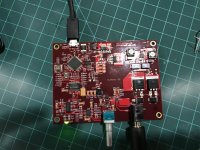
I see some quick hacks on the PCB. Did you find any faults with the design?
PS. Your Altium schematics are top notch. I like how clear and thought out they are.
No issues with board, I wanted to test it with and without the Buffer between the OPA1622 and the Pot, the pic was taken while I was testing that.
The other thing was the In-rush Resistor is currently jumped out because i selected a pretty crappy MOSFET after looking again, so the voltage drop was causing issues, I have already selected a new MOSFET to drop in.
The other various wires and such you see are Test Points i soldered in for scope probes etc.
I do plan on a second revision to correct a few minor things such as swapping the filter inductor and the fuse on the +5V bus. I will post the new revision of the schematic when it is completed, Ive got some other projects I am working on at the moment that are taking up my time.
Hi dmgash,
Great project! How did you get the I2S mode to synchronize between the XMOS chip and the DAC? Meaning, when you play a 16-bit file, does the XMOS output 16-bit I2S, and would you then need to command the DAC to change its format? Or does it always use a constant bit depth?
Great project! How did you get the I2S mode to synchronize between the XMOS chip and the DAC? Meaning, when you play a 16-bit file, does the XMOS output 16-bit I2S, and would you then need to command the DAC to change its format? Or does it always use a constant bit depth?
- Status
- This old topic is closed. If you want to reopen this topic, contact a moderator using the "Report Post" button.
- Home
- Source & Line
- Digital Line Level
- USB DAC PCM1794A, OPA1622