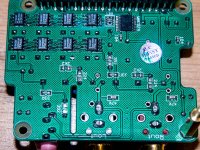
Hi, need some help in tweaking the passive I/V for the Teradak 8 x TDA1387 for Rasberry Pi. The dac in stock form sounded rather pleasant but has a lay back roll off high sound. I have traced the I/V output as below and welcome any ideas on how to improve it.
First this dac is the first one I have seem that uses an inductor directly at output to filter high fz noise. I think the 1mh value is a bit high and a cause for the roll off high and so I replaced the 1mH inductor with a much lower value 16uH Coilcraft that I have on hand and the high frequency seem to improved, but I don't think this is the optimal value.
The 500 ohm I/V resistor I think is too high. For one dac I think 2.7k I/V resistor is required, so for 8 dac around 330ohm might be more appropriate (pls correct me if I am wrong)
TIA")
TDA1387 dac
=> I/V resistor 500 ohm
=> RC to ground 33R +3.9nf (square blue cap on board)
=> Inductor (marking 103)
=> RC to ground 2.7k + 0.22uf (round blue cap, but resistor label 2.2k)
=> Nichicon BP 10uf for coupling
=> smd cap (label 47k) resistor 4.7K piggy back with 4.7nF smd cap
First this dac is the first one I have seem that uses an inductor directly at output to filter high fz noise. I think the 1mh value is a bit high and a cause for the roll off high and so I replaced the 1mH inductor with a much lower value 16uH Coilcraft that I have on hand and the high frequency seem to improved, but I don't think this is the optimal value.
The 500 ohm I/V resistor I think is too high. For one dac I think 2.7k I/V resistor is required, so for 8 dac around 330ohm might be more appropriate (pls correct me if I am wrong)
TIA
TDA1387 dac
=> I/V resistor 500 ohm
=> RC to ground 33R +3.9nf (square blue cap on board)
=> Inductor (marking 103)
=> RC to ground 2.7k + 0.22uf (round blue cap, but resistor label 2.2k)
=> Nichicon BP 10uf for coupling
=> smd cap (label 47k) resistor 4.7K piggy back with 4.7nF smd cap
Attachments
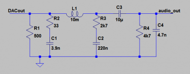
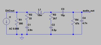
Would it be possible to draw up a schematic of the output section? I can't follow along well enough from the textual description to picture what's going on. For example 'RC' means R and C in series or in parallel?
<later> Added schematic - do I have it correct?
<later> Added schematic - do I have it correct?
Attachments
Last edited:
Would it be possible to draw up a schematic of the output section? I can't follow along well enough from the textual description to picture what's going on. For example 'RC' means R and C in series or in parallel?
Both RC is in series to ground. I know snubber is good after a transfromer, but not sure for inductor.
The last part with 47K is connected piggy back in parallel to ground.
Would it be possible to draw up a schematic of the output section? I can't follow along well enough from the textual description to picture what's going on. For example 'RC' means R and C in series or in parallel?
<later> Added schematic - do I have it correct?
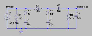
Thank you for the work, that is exactly the circuit except resistor near output is 47K instead of 4.7k.
You have also corrected my inductor value which is really 10mH.
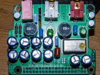
For the power supply, the 8 caps 1000uf/6.3V (looks like the general purpose Panasonic type) above is for the Vref pin whereas each of the Vdd only get a measly 0.1uf (as labelled) next to chip. I also measure only 4.65V for Vdd feeding from my Pi3 power. I wonder how much improvement if I power the dac with a good 5v separately.
Last edited:
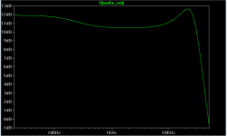
Here's the FR response plot, after I amended the output R to 47k. This change increased the peaking at the top end, so that aspect is going to be sensitive to loading in the pre/amp connected to this.
I agree with your comments re the 500R I/V resistor. The simulation shows for 8mA there will be 4V peak, this exceeds the output compliance range of the DAC. I will look at getting it down to 3V which would be a comfortable swing. There is also the small issue of the bass boost....
I agree with your comments re the 500R I/V resistor. The simulation shows for 8mA there will be 4V peak, this exceeds the output compliance range of the DAC. I will look at getting it down to 3V which would be a comfortable swing. There is also the small issue of the bass boost....
Attachments
Last edited:
Here's the revised version - input resistor reduced to 390R and 220nF increased to 2.2uF. This latter change moves the bass boost down in frequency so as not to affect the audio band.
Seeing as the 10mH inductor looks to be a cheap bobbin wound kind, it would pay to keep it well away from external mag fields (like mains transformers) or you'll pick up hum. On second thoughts, take that back - a closer look and they may well be screened. I shall look them up.
Seeing as the 10mH inductor looks to be a cheap bobbin wound kind, it would pay to keep it well away from external mag fields (like mains transformers) or you'll pick up hum. On second thoughts, take that back - a closer look and they may well be screened. I shall look them up.
Attachments
Last edited:
Here's the FR response plot, after I amended the output R to 47k. This change increased the peaking at the top end, so that aspect is going to be sensitive to loading in the pre/amp connected to this.
I agree with your comments re the 500R I/V resistor. The simulation shows for 8mA there will be 4V peak, this exceeds the output compliance range of the DAC. I will look at getting it down to 3V which would be a comfortable swing. There is also the small issue of the bass boost....
Thanks for the simulation. With a 10mH inductor in path, what causes the raising responds toward the higher treble?
Is this EQ'ed responds required for the tda1387. I know the tda1543 will need it. The tda1387 datasheet shows only a simple opamp filter with 1.5nf.
BTW, what software generates the simulation, maybe I can learn something from it. Thanks.
Also, for the I/V resistor, I have tried 270R (KOA carbon film) and 100R (Vishay s102), both is better than the original 500R and my set up has enough gain to accommodate the low output. How low resistance can I go for optimal output?
Link is from dac maker with layout and photos. I post the layout for easy reference from web.
DAC TDA1387*8 based I2S HiFi Audio decoder module for Raspberry PI B+ board
DAC TDA1387*8 based I2S HiFi Audio decoder module for Raspberry PI B+ board
Attachments
With a 10mH inductor in path, what causes the raising responds toward the higher treble?
Good question - the 10mH together with the 4.7nF form a 2nd order low-pass filter. 2nd order filters can have varying response due to differing amounts of damping - an underdamped filter behaves just in this way with a peak at the corner frequency. This peak is desired when the DAC is being used NOS (i.e. at 44k1 output sample rate) because NOS DACs are inherently subject to 'NOS droop' - a roll off that reaches -3.2dB by 20kHz. With higher sample rates this peak isn't required though 88k2 still needs a much smaller peak to get a flat response.
Is this EQ'ed responds required for the tda1387. I know the tda1543 will need it. The tda1387 datasheet shows only a simple opamp filter with 1.5nf.
Quite possibly the datasheet writers assumed it would be used with a digital oversampling filter (8X) and so did not need any EQ.
BTW, what software generates the simulation, maybe I can learn something from it. Thanks.
You can download it here - Linear Technology - Design Simulation and Device Models
Also, for the I/V resistor, I have tried 270R (KOA carbon film) and 100R (Vishay s102), both is better than the original 500R and my set up has enough gain to accommodate the low output. How low resistance can I go for optimal output?
There isn't a lower limit though if you want to maintain the same FR you should increase the 3.9nF in proportion to the reduction of your resistor. So for example increase to 20nF if you're using 100R. The 33R also should be reduced to maintain the same ratio with the I/V resistor.
I'll have a look at increasing the damping of the filter - that way you'll get the benefit of the rejection of images at higher frequencies but not have the rising HF response needed for NOS eq. I think its going to be simply tweaking a resistor value....
Attached the revised schematic - I took it that you'd settle on 100R for the I/V resistor and adjusted the other values accordingly. It looks impressively flat now
Attached the revised schematic - I took it that you'd settle on 100R for the I/V resistor and adjusted the other values accordingly. It looks impressively flat now
Attachments
Last edited:
Is there another way around this ?
'This' means the I/V stage or the filtering stage? Or both?
Improving on passive I/V isn't possible, the next step up is going to active I/V so as to present a lower impedance to the DAC's current source outputs. By 'active' though I don't mean opamps rather a discrete transistor circuit.
- Status
- This old topic is closed. If you want to reopen this topic, contact a moderator using the "Report Post" button.
- Home
- Source & Line
- Digital Line Level
- Improving passive I/V for Pi dac 8 x TDA1387