Evening all
I have been collecting the BOM and eagle cad design for homemade PCBs for a multi parallel TDA1541a NOS dac using the TNT-Convertus model (2 chips but maybe 4 (have sourced 3 and may stop there). Output will be tube stage.
At the moment I have the standard 3 regs from the TNT schematic serving each chip. I am now wondering about using SuperTeddyRegs as I already have 2 of his boards to hand.
Is it possible to run both (or 4 chips) from the same STR?
Will going to multiple chips defeat the purpose of having super regulators?
I have planned an arrangement of PCBs in a vertical stack like in the Cambridge Audio CD3 or DAC3. So I could interleave the STR boards between the dac boards with the Vout wire going out the "top" to one chip and another from the "bottom" going to the other chip so the power lines are going the shortest possible distances.
e.g.. shown for 4 dacs, only 1 iteration if 2 dacs
dac str dac dac str dac
|<---|--->| |<---|--->|
----------------------------------- base pcb which will carry parallel connections
Thank you for your comments
Last edited:
Evening all
I have been collecting the BOM and eagle cad design for homemade PCBs for a multi parallel TDA1541a NOS dac using the TNT-Convertus model (2 chips but maybe 4 (have sourced 3 and may stop there). Output will be tube stage.
At the moment I have the standard 3 regs from the TNT schematic serving each chip. I am now wondering about using SuperTeddyRegs as I already have 2 of his boards to hand.
Is it possible to run both (or 4 chips) from the same STR?
Will going to multiple chips defeat the purpose of having super regulators?
I have planned an arrangement of PCBs in a vertical stack like in the Cambridge Audio CD3 or DAC3. So I could interleave the STR boards between the dac boards with the Vout wire going out the "top" to one chip and another from the "bottom" going to the other chip so the power lines are going the shortest possible distances.
e.g.. shown for 4 dacs, only 1 iteration if 2 dacs
dac str dac dac str dac
|<---|--->| |<---|--->|
----------------------------------- base pcb which will carry parallel connections
Thank you for your comments
Have you not considered dual differential configuration.
You need one of Iancanada's I2Stopcm boards which provides the necessary dual simultaneous outputs for the dacs from the I2S signals, as well as reclocking them.
For my I/V converters I am using 4, AD844 current feedback opamps driving a pair of Sowter transformers as the 'output stage as they have a 'gain' of 5x.
This is ample to drive my Quad 405 via an Alps pot.
I am using low noise discrete regulators from Dexa (pin compatible with 78xx type)
Have you not considered dual differential configuration.
Thanks batteryman.
I'll need to read more about this approach.
So far I have made design decisions based on my skill/understanding level - I want to make the pcbs myself as far as possible. Also I don't have gear that accepts balanced inputs (except for a Chord power amp I was recently gifted) - I understand this dual differential treatment provides a balanced output? And because the rest of my kit is not particularly high-end I worry about that law of diminishing returns.
I've recently been adding a DEM clock sync to this project as well.
Dem reclocking is on my list as well, but there are several ways to do it.
The differential to single ended conversion is done by the transformers, which also have some lp filtering and of course common mode noise & rubbish cancels out. The 5:1 step up means no additional preamp is needed so avoids the psu & hardware of a valve output stage, but they are not a cheap option.
DAC OUTPUT TRANSFORMERS
You can connect them direct to the dacs across an I/V resistor and I was using this method, but a brief try using a single dac and an AD844 supplying the transformer produced more solid, more gutsy bass & lower midrange.
Once I've fitted Iancanada's board I'll probably try them connected directly again - I am trying to avoid active devices in the audio signal path.
The suggestions by batteryman are good. If you don't use a differential configuration, multiple DAC chips don't have any technical advantage than a single chip.
The ad844 is able to produce sparkling sound from top to bottom but it work best with a buffer at the output.
I am considering an OPA1632 differential opamp connected to pin 5 of the pair of 844s on each channel. Then the transformer across the outputs.
I think the reason the transformers weren't ideal connected directly to an i/v resistor is because they really need driving from a much lower impedance source.
Evening all
I have been collecting the BOM and eagle cad design for homemade PCBs for a multi parallel TDA1541a NOS dac using the TNT-Convertus model (2 chips but maybe 4 (have sourced 3 and may stop there). Output will be tube stage.
Might a collaboration be possible to share the pcb manufacturing costs? Should be possible to design a semi-universal 1541 nos dac pcb and I was thinking of designing my own (I have Labcentre's Isis/Aries schematic capture / pcb software which produces the Gerber files.)
My requirements are for differential working in simultaneous mode, I2S inputs with attenuators, 78xx pin compatible low noise regulators, dem clock derived from bck.
Preferably no smd parts. (the OPA1632 is soic and I can solder these)
The analogue section need not be on the same pcb (might be better if it wasn't) but if so, this would use 4x AD844, 2x OPA1632, +- 15v supplies with own regulators.
Might a collaboration be possible to share the pcb manufacturing costs?
Hi batteryman
Sorry just saw this invitation in your post last month.
Thanks for the offer. I don't think I am quite in the same league as your plans - yet! I am happy being low-tech at the moment with making my own boards and following the basic implementation that I have been settling on - need to start somewhere and though i know that I am making some design choices that are based on outmoded thinking and I will not end up with the ultimate on the first attempt, there will always be a next project to aspire to.
Best
Clayton
Hi batteryman
Sorry just saw this invitation in your post last month.
Thanks for the offer. I don't think I am quite in the same league as your plans - yet! I am happy being low-tech at the moment with making my own boards and following the basic implementation that I have been settling on - need to start somewhere and though i know that I am making some design choices that are based on outmoded thinking and I will not end up with the ultimate on the first attempt, there will always be a next project to aspire to.
Best Clayton
Yes everyone needs to start somewhere and I will eventually get round to designing my dual differential pcb later this year. I bought a pair of bare 1541 pcbs from Ebay but haven't had time to wire them up. At £13 a pair with on board psu, they were cheap enough for experimenting with but I could see where there was scope for improvements in the design and layout.
Ian
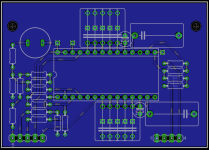
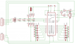
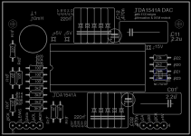
PCB critique please
Still working on this project. And haven't reviewed this thread for a while and now that I just have I see plenty of good comments that would benefit more attention.
However, must put my toe in the water and ask for feedback on the attached PCB design. Using attenuation and DEM reclock from ECDesigns post #2748.
Chip will be fed from separate pcb of same size containing multiple iterations of superegs in a vertical sandwich as per my first post.
The space for decoupling caps is tight/overlapping as I am using orange drop type capacitors and will alternate their placement top and bottom - even with the soldering just on one side I should be able to solder them all if I do them in the right order.
GND_A is the bottom layer
GND_D is the top layer
Using Eagle I was trying to make additional pad/holes to allow a small format capacitor - I used an extra pad on the schematic and so it appears on the screen print - is there a different way to do this to allow multiple component choices in the same spot?
All and any help much appreciated.
I know that there will be suggestions for different DEM clock or DAC implementations and they are always interesting to read. However, I am wanting to also better my PCB design skills so please bear that in mind.
Best to all and advance thanks
Attachments
Which dem decoupling caps are you using? Thru hole or smd?Still working on this project. And haven't reviewed this thread for a while and now that I just have I see plenty of good comments that would benefit more attention.
However, must put my toe in the water and ask for feedback on the attached PCB design. Using attenuation and DEM reclock from ECDesigns post #2748.
Chip will be fed from separate pcb of same size containing multiple iterations of superegs in a vertical sandwich as per my first post.
The space for decoupling caps is tight/overlapping as I am using orange drop type capacitors and will alternate their placement top and bottom - even with the soldering just on one side I should be able to solder them all if I do them in the right order.
GND_A is the bottom layer
GND_D is the top layer
Using Eagle I was trying to make additional pad/holes to allow a small format capacitor - I used an extra pad on the schematic and so it appears on the screen print - is there a different way to do this to allow multiple component choices in the same spot?
All and any help much appreciated.
I know that there will be suggestions for different DEM clock or DAC implementations and they are always interesting to read. However, I am wanting to also better my PCB design skills so please bear that in mind.
Best to all and advance thanks
You might find it difficult to find any thru hole types larger than 220n that are thin enough to stack side by side ie 2.5mm thick.
Ian
Which dem decoupling caps are you using? Thru hole or smd?
You might find it difficult to find any thru hole types larger than 220n that are thin enough to stack side by side ie 2.5mm thick.
Ian
I have drop type MKP caps for the 220n, tants for 470nf and then PPS for 2.2uf on MSB. I plan to mount alternating both sides of the board - I've mocked it up and have room and the nature of the caps allows one to get a solder iron under them to solder at the top of the lead. My boards will be mounted vertically. If I go in order from LSB to MSB by the time I get to the PPS caps on MSB that go flush to the board I will be able to solder them normally from the bottom of the board.
Cheers
Clayton
If I may Clayton, you must treat the TDA as an analog stage.
Been tweaking the living day lights out of my AYA & this is my
conclusion. It's very sensitive to PS tweaking for the 3 power
lines. So much so that even caps used be it main or decoupling
have great influence to SQ. This is my 2 cents, so design the
board to be easily tweak
Cheers
Been tweaking the living day lights out of my AYA & this is my
conclusion. It's very sensitive to PS tweaking for the 3 power
lines. So much so that even caps used be it main or decoupling
have great influence to SQ. This is my 2 cents, so design the
board to be easily tweak
Cheers
Am curious about what effect the 220n will sound like.
Apparently Arcam I think were the only guys using this
value
I recently acquired an Arcam Alpha DAC board (it is NOS natively) as a stop-gap on the way to building the 4x tda. Was going to do some testing with it to finalise my choices (e.g. Different I/V = SRPP or Nelson D1 and others?; different receivers = CS8214 w or w/o attenuation vs other receivers) Would be a good opportunity to also test some different sizes and types in Dem decoupling. I based my choices (5x220n film, 1x470n tant, 1x2.2u PPS = per side (Might not be able to get the 2.2uPPS on the Arcam board - haven't had the time yet to play) on the overview Lukas Fikas has made of the various implementations for his Lampizator pages. I see from your other threads you are concerned to get to optimum capacitance and care not to add capacitance just for the sake of it.
I see you flying the Indonesian flag. I am moving to Jakarta in a couple of months! Are there local meets? Are Sinar Baja drivers readily available locally for retail purchase?
Forgot, even the type of regs used affects its SQ.
For this dac it's not just about low noise regs.
Cheers
Just ordered some Newclassd UWB regs from Partsconnex to use as they are currently selling these out at >50% discount as Lars has just released a new version
Your point about PS choices is taken. With this test board I also have a couple of different style/size trafos to try - Toroid and EI core. I have looked a lot at the TNT Audio model with lots of capacitance - which was the direction I was heading but will try with both "just enough" and "overkill"
Thanks for taking time to comment
Last edited:
Indo is a huge country with too many islands.
Unfortunately I dont live in JKT, Im in an island
call Batam which is about an hours ride on ferry
to Singapore. We should catch up sometime when
your in Indo. I believe there's a small active group
of diyers in JKT. Stay away from toriods pls, used
it once & never again. Don't like its sound.
I always use EI, if you can get split bobbins better
still. Lastly beware of the traffic jams in JKT ya
horrid to the max but might help one to improve
patients. Lol
Cheerd
Indo is a huge country with too many islands.
Unfortunately I dont live in JKT, Im in an island
call Batam which is about an hours ride on ferry
to Singapore. We should catch up sometime when
your in Indo. I believe there's a small active group
of diyers in JKT. Stay away from toriods pls, used
it once & never again. Don't like its sound.
I always use EI, if you can get split bobbins better
still. Lastly beware of the traffic jams in JKT ya
horrid to the max but might help one to improve
patients. Lol
Cheerd
Very presumptuous of me to assume you live in the big durian - I look forward to visiting a few of those islands you mention. Sounds like it might be easier to visit with you if I am in Singapore! Thanks for your comments on trafo types for Digital - I have read that before.
What kind of minimum VA would you suggest ? If I run each of the +5 =5, -15 rails from their own trafo? In data sheet max current range for 3 Vdd is 35-50mA. Split bobbins are nice but from what I can source easily I can only get smallish ones e.g.. 6va
- Status
- This old topic is closed. If you want to reopen this topic, contact a moderator using the "Report Post" button.
- Home
- Source & Line
- Digital Line Level
- Parallel TDA1541a DAC using SuperTeddyRegs