I compared the 22MHz PN graphs what Andrea posts, the unshielded-shielded and the LDO-battery versions, I think there's no significant difference in PN and no necessary these options anyway.
What do you think?
Although there are no big difference (slightly better at 10 Hz from the carrier) I suggest to power with batteries all the digital to analog conversion chain (oscillators and DAC) to decouple them from the main AC.
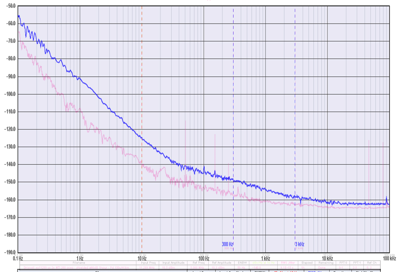
The close-in performance between 11.2896 & 22.5792 is quite huge. I was expecting 6dB drop in PN, but it's not. (20dB at 1Hz!)
I dont know the differences in circuit implementation between 5MHz and 22MHz, but I've encountered such results due to the increased ESR of the 22MHz crystal...
Without further details, I'm not saying that this is the case here but its a possibility...
A higher ESR does not mean a lesser Q in crystals. It still
depends on the C1 / L1 ratio. In fact, in a Butler or Driscoll
the emitter / source resistance != 0 does less harm to the
operating Q.
I was not referring to the impact on ESR / Q but while higher ESR increases the local Emitter feedback of the Hartly /Driscoll (a good thing) but higher ESR also INCREASES the noise just as increasing Emitter degeneration does....
This comes back to an earlier discussion we had, is the Emitter DC FB path (this thus forms part of the XO transistors Close in phase noise "circuit") via the paralleled inductor (which I claim it is) - on the other hand the noise contribution of the Crystal ESR MUST factor in the oscillators phase noise - you cannot introduce series resistance without also introducing noise - above absolute zero any resistance is noisy, so its common knowledge that lower resistance = lower noise.
Applying this logic, Lower Crystal ESR must equate to lower thermal noise?
If this is not the case, then I'd be happy to understand why
")
It's 7am here and I'm still sleeping, but at -150 dBc we are already
way above the thermal noise, including the Leeson effect that
produces a 10 dB/decade rise from the flat noise of the sustaining
amplifier.
And, feeding the assumed 2 Ohm emitter impedance, the signal
is from a current source effectively, so it's the noise CURRENT
that counts, really. The emitter Z shorts all of the crystal R's voltage
noise.
BTW among 100s of 100 MHz crystals, we found only 10%
that were top notch, in the same oscillator and close to the carrier.
And we ordered them with extra extra lapping etc for extra extra €,
nothing did help. Not top notch == 20 dB worse close-in.
(day-time job) We have no idea why.
I got the idea to build symmetrical notch filters around 100 MHz
to put the other 90% to use; the xtals are in the drawer after all for free.
Last edited:
Feeding the assumed 2 Ohm emitter impedance, the signal is from a current source effectively, so it's the noise CURRENT
that counts, really. The emitter Z shorts all of the crystal R's voltage noise.
I'm alittle lost here - are you referring to the "assumed 2 Ohm emitter impedance" of Emiiter "DC / LF" path formed by the paralleled inductor? I believe that this will impact the "Sustaining" amplifier circuit noise performance - BUT is the Crystals ESR REALLY out of the circuit when considering the Crystals inherent PN contribution? - I'm really not so sure.
BTW among 100s of 100 MHz crystals, we found only 10% that were top notch, in the same oscillator and close to the carrier.
And we ordered them with extra extra lapping etc for extra extra €, nothing did help. Not top notch == 20 dB worse close-in. (day-time job) We have no idea why.
I've given up on "Special crystals" and just hand select out of large numbers of far cheaper standard quality parts from China!!! for most applications this is ok (I'm not suggesting anyone would consider this for space applications)!!!
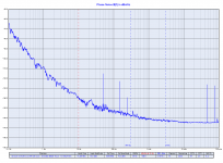
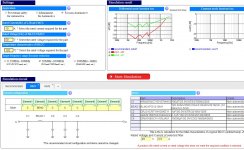
The phase noise plot of the new Driscoll oscillator without the oven with the Laptech Sc-Cut 3rd overtone crystal at 11.2896 MHz.
The result is -140 dBc at 10 Hz from the carrier and RMS Jitter around 9 femto Seconds.
.. Looks quite impressive, Andrea (& Co.) ... no stress (!) but the latest SC-cut curves you have posted make me wonder what a 5.6 MHz crystal would look like with an oven and a clock multiplier at various frequencies .. am thinking that it could be very interesting to see ... & again thanks for doing this to you (& your collaborators) ... ;-)
@gerhard:
Hmmm ... looks like one has to win a bit in the lottery ... Do you know if this variation is associated with certain manufacturers, or ... ?Not top notch == 20 dB worse close-in.
Cheers,
Jesper
I'm alittle lost here - are you referring to the "assumed 2 Ohm emitter impedance" of Emiiter "DC / LF" path formed by the paralleled inductor? I believe that this will impact the "Sustaining" amplifier circuit noise performance - BUT is the Crystals ESR REALLY out of the circuit when considering the Crystals inherent PN contribution? - I'm really not so sure.
In the Driscoll oscillator, the crystal is between GND and the emitter of lower
transistor. The second transistor is the usual cascode.
The input impedance at the emitter of the lower transistor is 1/gm and with
enough emitter current that is a few Ohms at most. That is semiconductor
physics and does not even depend on the transistor, give or take same
parasitics. With FETs this resistance is larger. gm = 30 mS or so for
good small signal FETs --> 33 Ohms. 33R in series to 66R of the crystal
will reduce Q from 1Meg to 660K, a bad thing. For a fundamental AT cut
with Rser = 20 Ohms that would be a disaster. The difference between
crystal Q and operating Q.
BJTs are the better choice here, also for their lower 1/f corner.
When the crystal had 10KOhm, it would be even less impressed by the FET's
33 R. (wild assumption, the 10k). It's thermal voltage noise would be huge,
but still shorted by the parallel 2 or 33 Ohm.
Last edited:
I dont know the differences in circuit implementation between 5MHz and 22MHz, but I've encountered such results due to the increased ESR of the 22MHz crystal...
Without further details, I'm not saying that this is the case here but its a possibility...
In order to clarify: the oscillator circuit is the same, only a few components have been changed according to the different crystal frequency (the feedback tank and so on).
The 3 crystals are obviously a bit different:
- 5.6448 MHz Sc-Cut 3rd overtone, average Q around 2.2M, average ESR around 97 ohm, average motional capacitance around 0.127 fF
- 11.2896 MHz Sc-Cut 3rd overtone, average Q around 1.1M, average ESR around 85 ohm, average motional capacitance around 0.150 fF
- 22.5792 MHz Sc-Cut 3rd overtone, average Q around 500k, average ESR around 38 ohm, average motional capacitance around 0.37 fF
There are great differences in the Q of the crystals, and also a big difference in ESR between the 22.5792 MHz and the other 2 crystals.
Since in the Driscoll oscillator the crystal stands between the emitter and ground, at the same emitter current, the greater the ESR of the crystal the greater the loaded Q of the circuit.
The ESR of the 5/11 MHz crystals is more than double the ESR of the 22 MHz. This maximizes the loaded Q of the 5/11 Mhz crystals, that have very similar ESR, penalizing the loaded Q of the 22 MHz crystal.
Highest unloaded Q and higher ESR of the crystal help a lot to maximize the loaded Q of the Driscoll oscillator circuit.
Theoretically this strongly affects the close in phase noise.
Obviously, one can increase the emitter current to lower the emitter impedance, but there is a limit beyond which the circuite becomes instable (gain, drive level of the crystal and so on). We found that the best compromise for the 22.5792 MHz crystal is a drive level around 100 uW (decreasing the ratio of the transformer in the collector circuit from 16:1 to 8:1).
That's the reason I suggest to start anyway from a crystal at a frequency around 5 MHz, where its Q reaches the maximum value.
I believe that a Driscoll oscillator with a 5.6448 MHz crystal followed by a pair of low phase noise frequency doubler will perform much better than the same oscillator using a crystal at 22.5792 MHz.
"That's the reason I suggest to start anyway from a crystal at a frequency around 5 MHz, where its Q reaches the maximum value.
I believe that a Driscoll oscillator with a 5.6448 MHz crystal followed by a pair of low phase noise frequency doubler will perform much better than the same oscillator using a crystal at 22.5792 MHz."
Interesting find Andrea congrats.
I believe that a Driscoll oscillator with a 5.6448 MHz crystal followed by a pair of low phase noise frequency doubler will perform much better than the same oscillator using a crystal at 22.5792 MHz."
Interesting find Andrea congrats.
Greetings for all,
I’m relative new in the clock design section, so I’ve my stupid beginner questions. If you feel some inspiration to answer please let me know…!
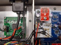
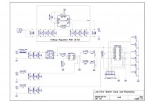
My setup contains the following elements (see photo):
- DIYinhk USB multichannel XMOS board
- my AK4458 multichannel DAC
- my reclocking board with Crystek CCHD-575 crystal, NB3L553-D buffer and PO74G374A logic gates, supplied from a TPS7A4700 3.3V regulator
The circuit is working good, although it is under testing yet. Before this setup I fed my DAC direct from a MiniDSP USBStreamer, without reclocking. The improvement is obvious: there are more microdetails, finer textures, the instruments are better focused and more separated. Brass instruments and violins are excellent detailed. Overall a more natural presentation, not so fuzzy like a typical "digital" sound.
But! After some experiments I must say that it’s not an easy task to design so a HF circuit correctly. Depending e.g. from the applied bypassing, the sound character changes too! By not adequate setup the higher transients can be too harsh/grainy and the midrange not so articulated. I’d like to make a little technical “walk around” here, to find and understand the optimal environment for such a circuit.
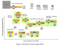
I’ve found some very helpful things by the manufacturer Murata:
Application Manual for Power Supply Noise Suppression and Decoupling for Digital ICs
https://www.murata.com/~/media/webrenewal/support/library/catalog/products/emc/emifil/c39e.ashx
SimSufring Noise Filter Design Support Tool
Noise filter design support tool
So, my questions in the first run:
- What are the exact bypassing/filtering requirements in terms of power supply impedance AND noise suppression level for the three parts (Xtal, buffer, gates)? /please remember, the Crystek clock has a built-in voltage regulator already as I know/ How many attenuation/impedance and up to which frequency is necessary?
- Why is the audio quality affected at all if different bypassing are applied? Is the jitter performance of the div. ICs changing with it?
- Does it make sense to supply the clock only from a separated voltage regulator e.g. to avoid unwanted HF back-coupling into the Potato-IC?
- Which I2S line(s) is/are the most important for the audio quality? If I follow my own logic, the data lines do not really playing any role because of the single serial bits will be stored in a DAC-register and switched free for the analog side by the LRCLK (or BCLK, I don’t know)…
- How important is really the reflection-free signal conditioning/terminating? What happens if I have some small overshooting in the different lines?
- What about the component quality? Some says that X7R caps “sounds” not so good…
Many thanks!
I’m relative new in the clock design section, so I’ve my stupid beginner questions. If you feel some inspiration to answer please let me know…!
My setup contains the following elements (see photo):
- DIYinhk USB multichannel XMOS board
- my AK4458 multichannel DAC
- my reclocking board with Crystek CCHD-575 crystal, NB3L553-D buffer and PO74G374A logic gates, supplied from a TPS7A4700 3.3V regulator
The circuit is working good, although it is under testing yet. Before this setup I fed my DAC direct from a MiniDSP USBStreamer, without reclocking. The improvement is obvious: there are more microdetails, finer textures, the instruments are better focused and more separated. Brass instruments and violins are excellent detailed. Overall a more natural presentation, not so fuzzy like a typical "digital" sound.
But! After some experiments I must say that it’s not an easy task to design so a HF circuit correctly. Depending e.g. from the applied bypassing, the sound character changes too! By not adequate setup the higher transients can be too harsh/grainy and the midrange not so articulated. I’d like to make a little technical “walk around” here, to find and understand the optimal environment for such a circuit.
I’ve found some very helpful things by the manufacturer Murata:
Application Manual for Power Supply Noise Suppression and Decoupling for Digital ICs
https://www.murata.com/~/media/webrenewal/support/library/catalog/products/emc/emifil/c39e.ashx
SimSufring Noise Filter Design Support Tool
Noise filter design support tool
So, my questions in the first run:
- What are the exact bypassing/filtering requirements in terms of power supply impedance AND noise suppression level for the three parts (Xtal, buffer, gates)? /please remember, the Crystek clock has a built-in voltage regulator already as I know/ How many attenuation/impedance and up to which frequency is necessary?
- Why is the audio quality affected at all if different bypassing are applied? Is the jitter performance of the div. ICs changing with it?
- Does it make sense to supply the clock only from a separated voltage regulator e.g. to avoid unwanted HF back-coupling into the Potato-IC?
- Which I2S line(s) is/are the most important for the audio quality? If I follow my own logic, the data lines do not really playing any role because of the single serial bits will be stored in a DAC-register and switched free for the analog side by the LRCLK (or BCLK, I don’t know)…
- How important is really the reflection-free signal conditioning/terminating? What happens if I have some small overshooting in the different lines?
- What about the component quality? Some says that X7R caps “sounds” not so good…
Many thanks!
Attachments
Imho it diserves its own thread, should ask the mods to move it as a new thread
It's ok here I think. But I'm suprised that nobody has answered yet...
@zarandok:
Hi ... I tend to agree with diyiggy that your questions may be more appropriate in a separate thread as they - as I read them - are less related to TWTMC but more of a general character in relation to decoupling, data transmission line optimisation, etc. And your focus, again as I read it, is the Crystek more than the TWTMC. This also means that I will just give a brief reply.
The questions you are asking IMHO are questions that partly throw some light on why audio may often be an art more than an exact science. Data line impedance choices determines undershoot/overshoot of a data line, which again feeds back to the PSU of the active elements involved, which again affects the choice of components, which again is affected by the more exterior design components like AC line filtering (regulators, capacitors, etc.).
In my understanding there is no single "right" choice but the individual designer may choose to focus on and optimise various aspects of the design. IMHO it is difficult - maybe impossible - to optimise everything because digital signals essentially go from ~ DC to light frequency (a pure square) and all real world components are frequency limited to some extent. Thus, choices and optimisations are a fact of the day.
I have listened to a good selection of same value components in the same digital PSU decoupling positions and my personal current choices are to optimise the decoupling capacitors (I don't use resistors in the PSU decoupling lines) for the main frequency to be decoupled. I.e. for a ~12 MHz decoupling frequency I would use a 100 nF capacitor. However, do note that long(er) tracks from the decoupling capacitor to the IC (and the IC's internal wire connection lengths - induction) may change the optimum value.
To this end my experience is that different manufacturers' SMD capacitors may sound quite different, and yes, also IME X7R based SMDs are not the best sounding (in general a bit "mushy", unclear, less dynamic, but can have a reasonably neutral tonal reproduction). I use Kemet's online capacitor tool to decide which capacitor has the desired frequency characteristic KEMET K-SIM: Capacitor Model Simulation Tool
I combine lower value SMD based capacitors with other capacitors to get a stable supply voltage.
Regarding data line transmission I tend to ever so slightly over-damp the transmission line. My notion is that since filtering of the digital signals in general is a challenge it is most feasible to not create more harmonics to be filtered by the decoupling components by under-damping the data line. Thus, very slightly over-damped. A helpful tool here has been Saturn's PCB design tool which can be downloaded for free (or a donation).
For PSU I in general use batteries due to their very low noise level and high current delivering capability.
To sum up: The questions you are asking IMHO takes personal experience and choice to answer. Yet, I hope that maybe my short reply may be of inspiration.
Cheers,
Jesper
It's ok here I think. But I'm suprised that nobody has answered yet...
Hi ... I tend to agree with diyiggy that your questions may be more appropriate in a separate thread as they - as I read them - are less related to TWTMC but more of a general character in relation to decoupling, data transmission line optimisation, etc. And your focus, again as I read it, is the Crystek more than the TWTMC. This also means that I will just give a brief reply.
The questions you are asking IMHO are questions that partly throw some light on why audio may often be an art more than an exact science. Data line impedance choices determines undershoot/overshoot of a data line, which again feeds back to the PSU of the active elements involved, which again affects the choice of components, which again is affected by the more exterior design components like AC line filtering (regulators, capacitors, etc.).
In my understanding there is no single "right" choice but the individual designer may choose to focus on and optimise various aspects of the design. IMHO it is difficult - maybe impossible - to optimise everything because digital signals essentially go from ~ DC to light frequency (a pure square) and all real world components are frequency limited to some extent. Thus, choices and optimisations are a fact of the day.
I have listened to a good selection of same value components in the same digital PSU decoupling positions and my personal current choices are to optimise the decoupling capacitors (I don't use resistors in the PSU decoupling lines) for the main frequency to be decoupled. I.e. for a ~12 MHz decoupling frequency I would use a 100 nF capacitor. However, do note that long(er) tracks from the decoupling capacitor to the IC (and the IC's internal wire connection lengths - induction) may change the optimum value.
To this end my experience is that different manufacturers' SMD capacitors may sound quite different, and yes, also IME X7R based SMDs are not the best sounding (in general a bit "mushy", unclear, less dynamic, but can have a reasonably neutral tonal reproduction). I use Kemet's online capacitor tool to decide which capacitor has the desired frequency characteristic KEMET K-SIM: Capacitor Model Simulation Tool
I combine lower value SMD based capacitors with other capacitors to get a stable supply voltage.
Regarding data line transmission I tend to ever so slightly over-damp the transmission line. My notion is that since filtering of the digital signals in general is a challenge it is most feasible to not create more harmonics to be filtered by the decoupling components by under-damping the data line. Thus, very slightly over-damped. A helpful tool here has been Saturn's PCB design tool which can be downloaded for free (or a donation).
For PSU I in general use batteries due to their very low noise level and high current delivering capability.
To sum up: The questions you are asking IMHO takes personal experience and choice to answer. Yet, I hope that maybe my short reply may be of inspiration.
Cheers,
Jesper
Last edited:
Hi Jesper,
thanks a lot! I'll study this things... Attached my actual schematic.
thanks a lot! I'll study this things... Attached my actual schematic.
A P.S. to my previous post: Two more sources that I have been using have been Johnson's High Speed Digital Design, and Henry Ott's Electromagnetic compatibility Engineering.
Cheers,
Jesper
Attachments
- Status
- Not open for further replies.
- Home
- Source & Line
- Digital Line Level
- The Well Tempered Master Clock - Building a low phase noise/jitter crystal oscillator