Looks both nice and right as far as I can tell, but I'm not qualified to comment on the finer details; that I leave to other, more capable eyes 🙂
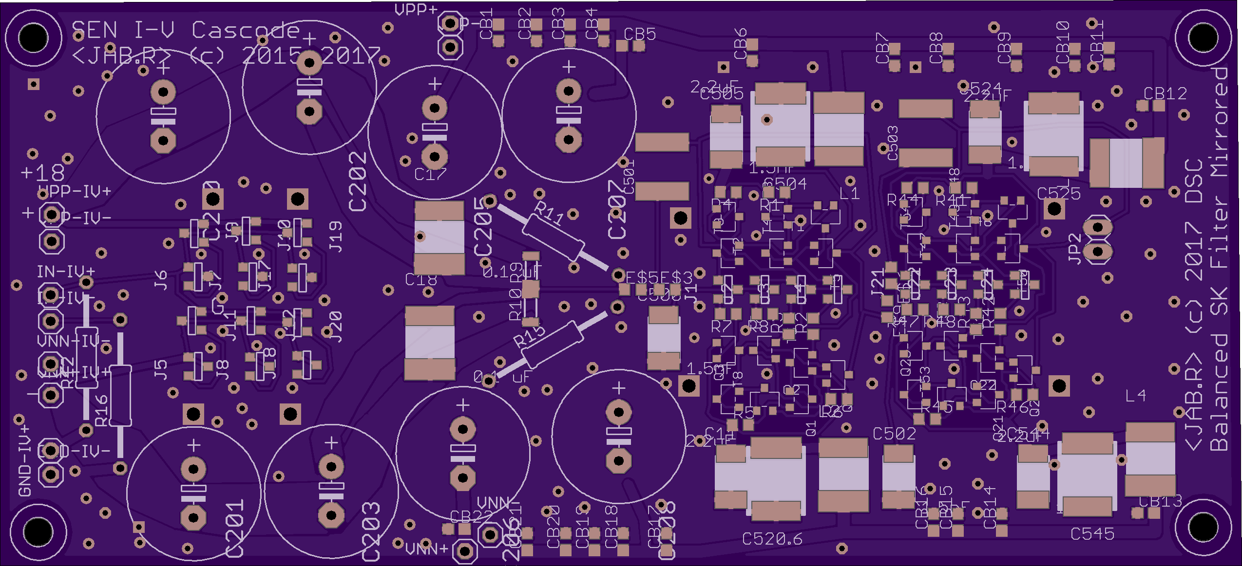
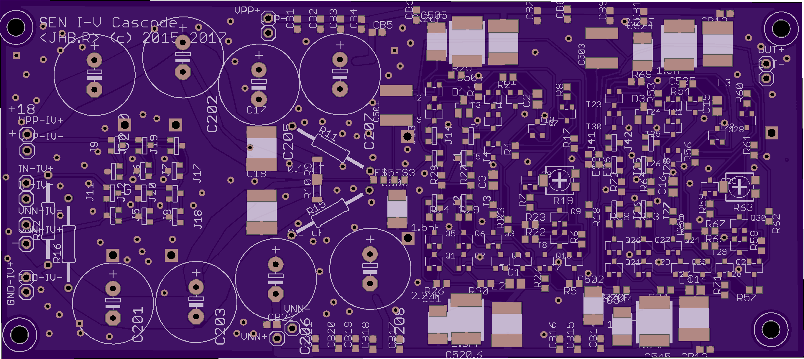
The balanced, mirrored, discrete cascoded JFet analog board:
OSHPark link to order boards (need 1/channel):
https://oshpark.com/shared_projects/TjK3dURD
OSHPark link to order boards (need 1/channel):
https://oshpark.com/shared_projects/TjK3dURD


jborden,
that pcb Is a real treat
thank you for your hard work
which DAC you will use - pcm1704 ?
what are power requirments for pcb
that pcb Is a real treat
thank you for your hard work
which DAC you will use - pcm1704 ?
what are power requirments for pcb
This is the analog board which goes with the Balanced, Clock optimized DSC board -- I've posted this on this thread and also to OSH park.
Power, yes, each SEN I-V uses a floating 18V supply and the filter section prob +/-12-18V (doesn't require floating)
In the power supply section, I posted a floating supply circuit which I'm building for this but a couple of 9v batteries are fine for the IV section.
Since the design is fully cascoded and discrete the exact voltage requirements aren't entirely strict.
Last edited:
Regarding PCM1704, yeah so outside the scope of the DSC DAC which is pure DSD but my own plans involve building an ARM/FPGA input section with the Xilinx Zynq SoC which will accept Ethernet in and convert to direct DSD and/or PCM depending on the input stream. The advantage of this approach is that it would output PCM in the format the 1704 accepts rather than I2S (for example)-- since its programmable no problem to reconfigure as needed.
Also insert multistage isolate/reclock between FPGA and DSC board
<JAB.R>
Also insert multistage isolate/reclock between FPGA and DSC board
<JAB.R>
Update on the Analog board:
SEN I-V BF862/J111 Cascode
SW-OPA SK Filter BF862/J111 Cascode "final version"
https://oshpark.com/shared_projects/WqGurTbd
SEN I-V BF862/J111 Cascode
SW-OPA SK Filter BF862/J111 Cascode "final version"
https://oshpark.com/shared_projects/WqGurTbd


Hello @jborden
do you have the schematics?
Yes, certainly however due to the way I've done this, the part numbers on the board I've supplied do not match the schematic.
The overall schematic -- I'm calling this version DSC1.2jb to avoid confusion with DSC2 that Jussi Laako plans to release at some point in the future:

http://www.diyaudio.com/forums/digi...inimalistic-iv-converter-188.html#post4961030:

http://www.diyaudio.com/forums/anal...screte-opamp-open-design-236.html#post3279329:

Last edited:
Thanks @jborden!
What is coming after filter section?
Do you finished your floating supply tests?
@nautiboy
Did you´ve more information about the post #371? FIR 32 bit + transformer = simple!
And why 8k06? Very difficult to get! I´m using 10k Vishay networks for riv 350R.
JP
What is coming after filter section?
Do you finished your floating supply tests?
@nautiboy
Did you´ve more information about the post #371? FIR 32 bit + transformer = simple!
And why 8k06? Very difficult to get! I´m using 10k Vishay networks for riv 350R.
JP
Thanks @jborden!
What is coming after filter section?
Do you finished your floating supply tests?
@nautiboy
Did you´ve more information about the post #371? FIR 32 bit + transformer = simple!
And why 8k06? Very difficult to get! I´m using 10k Vishay networks for riv 350R.
JP
My goal was to "jFet" the DSC1. It actually measures great and I think a terrific basic design. So balance and mirror and discrete but stays true to the DSC1. Trying to give that jfet "sound"
In this version, the op amps have their own output section ... alternatively could build a simpler jfet op amp and then add an output section.
I'm using 2 9V batteries in series for testing purposes ... very easy.
I divided the circuit into a digital and analog section. That does allow folks to mix and match if desired. There are designs other than the DSC1 which don't include a FIR as well as modifications to the FIR. I haven't seen a good enough analysis about why that is preferable. I understand the FIR in the DSC1 and am using.
I am using one "exotic" resistor for the I-V Riv because that's a critical part.
In other cases I've selected SMD parts that I have. In many cases they can be substituted within reason. Likewise the OP amps have a wider supply range (being discrete and cascoded)


There is an error in my original schematic for the digital side (that doesn't affect the board layout) -- I mentioned that I'm using CMOS V3.3 and the potato semi clock buffer & d-flop : those are PO74G74A (d-flop) and PO49FCT3807B (clock buffer) as well as the AHC series (not AHCT) shift registers i.e. 74AHC595 -- these are the CMOS version
I will post a corrected version later
I will post a corrected version later
Thanks @jborden!
Here first attempt for the OPA:
1 - GND Return
2 - IN-
3 - IN+
4 - VS-
5 - TRIM (external 2k)
6 - OUT
7 - VS+
8 - TRIM
JP
Looks really interesting ... are those 0201 components? This looks like a great package for folks who want to swap in the discrete OPA. What are your plans for building this?
DSC 1.2jb Digital Section Schematic
The corrected schematic (doesn't change the posted board except for the changing the labels on the ICs: TTL->CMOS versions).

The 74AHC595 parts are rated for minimum 80 Mhz (typical 120Mhz) at CMOS levels, so we should be good for DSD1024 and possibly DSD2048. That should be fine four our purposed -- I am hoping to do 16 channels of DSD1024 if I can optimize the Ethernet -> DSD with my FPGA. Not that this is needed, nonetheless...
The corrected schematic (doesn't change the posted board except for the changing the labels on the ICs: TTL->CMOS versions).
The 74AHC595 parts are rated for minimum 80 Mhz (typical 120Mhz) at CMOS levels, so we should be good for DSD1024 and possibly DSD2048. That should be fine four our purposed -- I am hoping to do 16 channels of DSD1024 if I can optimize the Ethernet -> DSD with my FPGA. Not that this is needed, nonetheless...
Last Version FIR32 bit:
- 0402 PANASONIC ERA-2A (8k06)
- DHVQFN16 74(AHCT, HC, HCT)595
Braining about thermal coupling W-OPA... suggestions welcome: I´m thinking about 3 metal sheets and two PA 3D printed clips?
Today: SEN I/V second attempt (pinning like AD844)
JP
- 0402 PANASONIC ERA-2A (8k06)
- DHVQFN16 74(AHCT, HC, HCT)595
Braining about thermal coupling W-OPA... suggestions welcome: I´m thinking about 3 metal sheets and two PA 3D printed clips?
Today: SEN I/V second attempt (pinning like AD844)
JP
Attachments


- Home
- Source & Line
- Digital Line Level
- Signalyst DSC1