Guys please don't use ceramic caps after the MIC regs. I would like to advise to use 4.7 uF tantalums before and after the regs. I was soldering 3 DACs yesterday evening and found that 1 uF X7R was mentioned in the BOM as an alternative. Please stick to the recommended tantalum caps.
MIC regs will oscillate with ceramic caps at their outputs !
MIC regs will oscillate with ceramic caps at their outputs !
Does that mean the Germans let you have your stuff? ")
JP, I wasn't totally clear about the alternate items. For some designs they represent upgrades. I get the impression this BOM is based more on availability from various vendors. Can you clarify?
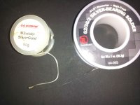
I'm sorting /confirming the remaining Mouser parts I got yesterday and should start soldering presently. I went with the Radio Shack silver solder. Big difference in size. Got a picture but the site seems to be having graphics/gallery problems at the moment. I'll try to post it later.
JP, I wasn't totally clear about the alternate items. For some designs they represent upgrades. I get the impression this BOM is based more on availability from various vendors. Can you clarify?
I'm sorting /confirming the remaining Mouser parts I got yesterday and should start soldering presently. I went with the Radio Shack silver solder. Big difference in size. Got a picture but the site seems to be having graphics/gallery problems at the moment. I'll try to post it later.
Another orientation question. C5, 7, 15, ..... are polarity marked. Data sheet does not indicate if that is the standard (-) marking for caps.
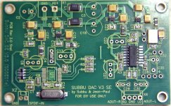
Hi we tried to pick parts that perform good but some are easier to find. We choose standard industrial parts generally except for caps which I first try out in prototypes. My 3 pieces V3 are all made with different caps. The BOM is something some of you ask for religiously. I never make BOMs as I choose caps myself. Take for instance the aluminium pearl caps which are hard to get. Have to admit the aluminum pearl caps were chosen by me as they are a worthy replacement for Black Gate caps. Since I stock both I also try both. Subbu made the BOM and sends me the other standard parts.
*tantalum caps always have the positive pole marked in opposite to electrolytic caps. Don't ask me why, it only gives confusion but it is a fact. So the + is the thick line left of the text on the cap*
Too bad the data sheet says nothing about that, it should be described. The electronic industry choose to deviate from a standard but fails to make it clear at least that is what AVX does in their data sheet.
And yes the Germans let me have my stuff after I promised to have my stuff sent over (next time) with a proper value statement of all parts that are inside.
Last edited:
 TNX
TNXThis is really embarrassing, but with great effort, I managed to loose the DAC chip for the DAC before I could get it on the board. I know it's here - just can't put my finger on it. Had it yesterday. 
I did note the chip I received with the boards did not match some of the numbers in the BOM. I'll order a new chip tonight - but want to make sure what was included in my kit wasn't a special series or die.
Mouser WM8804
I know it's here - just can't put my finger on it. Had it yesterday. I did note the chip I received with the boards did not match some of the numbers in the BOM. I'll order a new chip tonight - but want to make sure what was included in my kit wasn't a special series or die.
Mouser WM8804
Maybe it's not just me. I'm seeing U6 on the BOM I have listed as ES9023. The ES9023 is in place, but not at U6 - which is a five point pad similar to U3, 4, 5.
U1 is open and listed as WM8804 on the BOM, and is the part I received with the PCBs - I believe. That transceiver is what I misplaced and have ordered. Honestly, I didn't pay that much attention to the large multi-lead chips till assembly started.
So, does the BOM need some adjustments, or could I just have a version that doesn't reflect the final product? ---- or is it still just me ?????
I think that line on the BOM should read "U3-U5-U6, as I have one extra MIC5205-3.3.
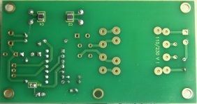
With the exception of U1 and U6, all the surface mount parts are soldered on the board. I'll wait till the site gets the graphics upload problems corrected and I can post a photo before I finish with the through-hole parts.
U1 is open and listed as WM8804 on the BOM, and is the part I received with the PCBs - I believe. That transceiver is what I misplaced and have ordered. Honestly, I didn't pay that much attention to the large multi-lead chips till assembly started.
So, does the BOM need some adjustments, or could I just have a version that doesn't reflect the final product? ---- or is it still just me ?????
I think that line on the BOM should read "U3-U5-U6, as I have one extra MIC5205-3.3.
With the exception of U1 and U6, all the surface mount parts are soldered on the board. I'll wait till the site gets the graphics upload problems corrected and I can post a photo before I finish with the through-hole parts.
Last edited:
Hi bcmbob,
I also noticed that the BOM has not the correct designators for all parts.
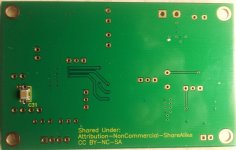
You can use the silk screen together with the Schematics PDF to put the right parts in the right place.
U3, 5 and 6 are the 3.3V regs and U4 is the 3.6V reg. U1 and 2 are obvious...
Br
Josch
I also noticed that the BOM has not the correct designators for all parts.
You can use the silk screen together with the Schematics PDF to put the right parts in the right place.
U3, 5 and 6 are the 3.3V regs and U4 is the 3.6V reg. U1 and 2 are obvious...
Br
Josch
I feel with you but I have not received boards & parts yet. I subscribed both GBs.
I'm patiently looking forward to it. The last time I soldered SMD was an AMP32 kit from 41HZ several years ago and my eyes are certainly not better these days. If I only manage to produce an ugly heap of burned solder I won't brag about it here
but I have not received boards & parts yet. I subscribed both GBs.I'm patiently looking forward to it. The last time I soldered SMD was an AMP32 kit from 41HZ several years ago and my eyes are certainly not better these days. If I only manage to produce an ugly heap of burned solder I won't brag about it here
I'll share a couple things I found on this go-round that may help:
Never work near the edge of your table or bench. Specially if you have carpet where dropped pieces can hide.
Identify the pads on the PCB and put sticky flux on them before you even open the package.
I open the small casings with the point of a utility blade directly over the PCB. Just lift the film from the side - don't cut into the container
I stopped trying to grab tiny things with pliers or tweezers. If the grip isn't good they can fly across the room in a heartbeat. Just move/slide them into position on the prepared pad with the blade point or a sharp pencil tip.
The best thing I've found to hold parts in position is surprisingly a long fingernail. The heat/solder time is so fast there is little chance to transfer heat to the nail. **Use at your own risk - works for me**
As JP stated - the 0.015"/0.39mm solder makes a world of difference. Cleaning the tip on almost every solder joint really helps carrying the minimum amount of solder to the work. Some spots have very little overhang on the pads. If available, I seems to work best to hold the SMD part in place, start at the pad edge and sweep the solder into or across the leads on the part.
It might be helpful to start with a couple medium to large surface mount parts just to get a feel for how your solder and tip combo operate. That helps build confidence for when you get to the ridiculously tiny pieces.
And of course - the best lighted magnifier system you can afford is a must. I use one of those goose-necks with a 5" lens and a doughnut florescent tube. Got mine from Harbor Freight for ~ $30 on sale. I'd be lost without it.
Last edited:
Maybe it's not just me. I'm seeing U6 on the BOM I have listed as ES9023. The ES9023 is in place, but not at U6 - which is a five point pad similar to U3, 4, 5.
U1 is open and listed as WM8804 on the BOM, and is the part I received with the PCBs - I believe. That transceiver is what I misplaced and have ordered. Honestly, I didn't pay that much attention to the large multi-lead chips till assembly started.
So, does the BOM need some adjustments, or could I just have a version that doesn't reflect the final product? ---- or is it still just me ?????
I think that line on the BOM should read "U3-U5-U6, as I have one extra MIC5205-3.3.
With the exception of U1 and U6, all the surface mount parts are soldered on the board. I'll wait till the site gets the graphics upload problems corrected and I can post a photo before I finish with the through-hole parts.
I never use BOMs myself as I follow schematics to PCB (hardcore approach
). So I know there are 4 regs of which one is 3.6 V and that's the one for the DAC chip. I know this is not standard nowadays and we must correct the BOM if it has errors. Will ask Subbu if I can have the latest version and we will correct it.Had to smile when I read about parts flying away and you don't find them anymore. Until you got new ones, then you see something tiny and shiny in the carpet...
You are right about using thin solder and cleaning the tip after a part is soldered. A wet sponge is the best. BTW I use tweezers made of material that can not be soldered to keep the part aligned (I think mine is made of titanium or an alloy). Then I solder one pin and push the part with a long fingernail and touch the same pin again with the Weller. Then the other pins.
The XO is a tough one on the final PCB. I personally think the footprint on the old boards was better but I got them soldered.The resistor array was a breeze, Subbu sent me a type that was much easier to fix than the type I used on the prototypes.
The gold finish looks good but it transfers heat too good
The tinned boards were easier to solder but I like the gold bling factor of the new ones.
Last edited:
Bob, a bit late now but you don't need to carry the solder with the iron bit to the smd component - if you tin the pads adequately first just place the component onto the pads, bit more flux if needed then heat the tinned pad and the solder will flow to the component contacts easily. Settle the component if needed.
You will have a perfectly flowed joint and the right amount of solder.
Good luck with your build
You will have a perfectly flowed joint and the right amount of solder.
Good luck with your build
Sounds like a better method. But as you say, a bit late as all the SMD parts are mounted on the PS board and only U6 and U1 are open on the DAC. I'll try it on those when they arrive - hopefully tomorrow afternoon.
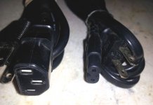
I hate to expose all my dumb moves to the entire world, but I neglected to order the biggest part in the project - the PS transformer. Guess I was thinking "small and tiny" and looked right past that big hunk of copper. Well, that's my story/excuse and I'm sticking to it.
Have to give Mouser their props though. I discovered the missing trani just moments after completing a combo order for a couple projects. They weren't open in the central time zone yet, so I popped off an email requesting it be added if possible. Several hours later I got a reply stating once my credit card was charged no changes could be made. They resolved the issue by voluntarily generating a new separate order, waived all shipping charges and sent them both off side by side. I think that's something special in today's business climate. A tip of the fedora to the folks at Mouser.
Last edited:
Here is a link to a video those building the MyRef FE amps are using. Dario has fewer SMD parts but the technique is the same. He did a nice job demonstrating with various sizes and shapes on his PCB Design.
There are a couple approaches as noted in post #34. You can check out the other videos in the sidebar there on the YouTube page. As stated, I suggest the fingernail as a better hold down tool once the part is in place. That's the real reason your mother always told you to stop biting your nails.
I have a few more photos but the diyAudio site upload function has been down since yesterday. I'll post them when it's fixed.
SMD Soldering Demo
Last edited:
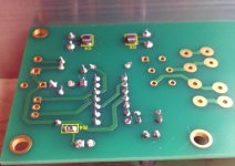
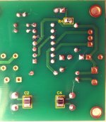
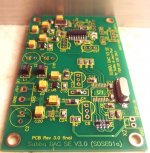
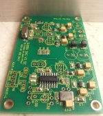
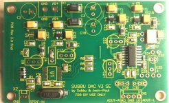
So Far - So Good, I hope.
These represent the progress to date. Might not be able to move on till Monday.
You will see some TH spots that appear to be missed or cold solder joints. I left them in because they didn't show up till after the board cleaning (Alcohol & Dow Bathroom Cleaner) was done. Care must be taken to make sure nothing is hidden by caked flux.
It's probably evident which pieces were done with the fat solder. Even with great care it can be tough to keep SMDs in line. I could make corrections, but don't want to use more heat unless absolutely necessary.
Duplicates are from different camera. The lint fibers come from the clean shoe brush used to polish the boards. Another pass of alcohol/toothbrush and they will be gone.
I'll give it a B+. What say you Mr. JP?
Attachments
-
 Solder.jpg64.6 KB · Views: 847
 -
 B1.JPG65.4 KB · Views: 247
 -
 20131108_182145.jpg96.4 KB · Views: 297
 -
 20131108_180256.jpg146.6 KB · Views: 300
 -
 20131108_175105.jpg78 KB · Views: 738
 -
 20131108_175215.jpg177 KB · Views: 759
 -
 20131108_175230.jpg180.5 KB · Views: 776
 -
 A2a.jpg615.5 KB · Views: 789
 -
 A2.JPG158 KB · Views: 375
Last edited:
- Home
- Source & Line
- Digital Line Level
- Build thread - building the Subbu DAC V3 SE