This evening I was experimenting with the idea of simply using the second stage of Rod Elliott’s P88. See figure 4 here (also attached):
High Quality Audio Preamp
So, in essence, you have a dac chip (AD1865 in my case) with a passive iv resistor (120R), which is then sent straight into BL and BR on the P88 pcb. Surprisingly, this works perfectly - far better than my tube AIKIDO, believe it or not! It is also great for experimenting with opamps (and easier on the wallet given you only need one dual opamp!).
The only queries I have are in relation to input impedance. Presumably the input impedance of the stage is determined by R6? Which would make it 15k. Rather low. Is there any need to modify the second stage circuit for RF filtering or impedance issues when used for iv purposes?
On another note, given the AD1865 has very little DC at the ouput of the DAC chip when used passively, I actually took out the 1uF capacitors at the output of P88. It was like lifting a thick veil, much more clarity. DC offset is only about 1 to 2 mv with OPA627 and OPA2211, ranging up to 4mV with AD825. Fine for use with any power amp, no caps in the signal path of the I/V stage!
Attachments
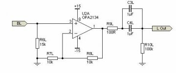
To keep offset values as low as possible, the impedance seen by the + input and
the - input of the op amp should be the same.
In the example above, they do not match.
The - input sees 5k and + input sees a little less than 120R.
If you reduce the feedback and gain resistors to 500R each, you should
get even lower offset figures.
You can leave the 15K input resistor in circuit, it will have little impact
on the 120R I/V resistor and protects the circuit should the 120R be dis-
connected while the circuit is on.
To get the lowest offset, the feedback and gain resistors should be 240R each.
The op amp would be driving 480R plus the input impedance of the next stage.
An LME49990 would probably sound pretty good here.
You could also bias the output of the op amp into class "A" by using a CRD with
a value of 2mA (you can experiment with this value).
The op amp would be driving 480R plus the input impedance of the next stage.
An LME49990 would probably sound pretty good here.
You could also bias the output of the op amp into class "A" by using a CRD with
a value of 2mA (you can experiment with this value).
Yes, R7 is the gain resistor and R8 is the feedback resistor.
The gain of this circuit is 2. By changing the ratio of R7 to
R8, you can have more or less gain as well.
CRD = Current Regulating Diode
The gain of this circuit is 2. By changing the ratio of R7 to
R8, you can have more or less gain as well.
CRD = Current Regulating Diode
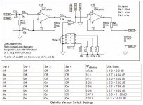
OK - the pcb itself has a switch for various gain settings (see attached pic).
Currently I have it set on "ON ON ON OFF" which gives an effective R7 of 3.47K. The dc offset on each channel with this setting is less than 5mV.
I'm not overly keen on de-soldering the R7 resistors as they're decent metal film takman types, and I've only got some standard 240R ones to replace them with (I'd pick one of the switches and leave the other three off).
Presumably making this change wouldn't actually affect the sound at all? Just the dc offset - which is already rather low?
Attachments
Ah, I see.
Yeah, I wouldn't bother changing the resistors.
You can still try the trick with the CDR on the output.
If you build your own board from scratch, you can use
the values above.
With the board you have, just use the lowest gain value
that provides enough output for you.
If you try the CRD, it goes from the op amp output to
the negative voltage rail.
You might have to make your own with a FET and resistor.
Here is a great article which explains it all pretty well.
Here is a great article which explains it all pretty well.
The lower resistor values will give you less noise.
Whether this is audible depends on the noise values
for the op amp.
I'd say it might be audible with headphones or a solid state power amp?
I'm using a tube power amp, so it's probably not a critical change
Hi, lordearl,
Matching the resistance of the two input networks so to minimize the input offset voltage depends on a given op-amp's input stage bias current. The smaller the input bias current, the smaller will be the benefit of matching input resistances. So, for a FET input op-amp, such as is the OPA627, matching the input resistance will, essentially, provide no improvement in D.C. offset. I suggest that you not worry about a 1 or 2 mv offset. Most of the cures seem worse than the disease. Particularly, if the cure is a low resistance feedback network, which will greatly increases the A.C. current demanded of the op-amp's output stage.
Just my two cents worth.
Just did some more testing and it appears that the DC is stemming from either the usb interface or the DAC, which is earlier in the audio chain.
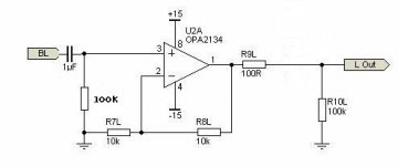
How about the attached for an improved schematic? The cap at the input will block and DC and the 100k should also raise the input impedance in order to allow for other options down the track (eg DAC with a transformer at the output stage).
How about the attached for an improved schematic? The cap at the input will block and DC and the 100k should also raise the input impedance in order to allow for other options down the track (eg DAC with a transformer at the output stage).
Attachments
- Status
- This old topic is closed. If you want to reopen this topic, contact a moderator using the "Report Post" button.
- Home
- Source & Line
- Digital Line Level
- Nice little opamp circuit for I/V stage