Sorry, I'm currently in a place with limited internet access and even more limited free time (organizing a youth gathering), so this will be short:
- keep in mind it was a few years ago... I lost most of the actual schematics (the one I posted is not a practical implementation, sorry for the confusion).
- I used the bc337-40 at the time because I had a bunch... might be worth trying to optimize the transistors used. I'd drop some of the diode-connected transistors in favor of leds.
- wrt oscillations: I didn't get any on scope but I had a highish Civ.
- as posted, current seems overkill for a pcm1795-6. I tested it on a pcm1798 but with lower currents.
- as far as I remember, chasing low Rin was the trend of the day, which explains it somehow.
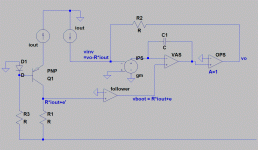
In the figure,
vinv = vo-R*iout
then IPS outputs current, multiplied vinv and gm.
If we regard whole the current flows miller capacitor,
since the inverting input of VAS is virtual shorted to vboot,
vo = (vo-R*iout)*gm/Cs+vboot
if we assume,
vboot = R*iout+e
here e is error voltage.
substituting,
vo = vo*gm/Cs-R*gm/Cs*iout+R*iout+e
arranging,
vo*(Cs-gm) = R*(Cs-gm)*iout+Cs*e
vo = R*iout + Cs/(Cs-gm)*e
= R*iout + e/(1-gm/Cs)
here,gm/Cs is apparently OPA's open gain and equal to loop gain.
When gm/Cs is sufficiently larger than 1,
it is able to be regarded e is suppressed by loop gain.
Since R*iout term is based on virtual short to vboot,
IPS supplies current to miller cap only error term.
If the e is 1% of R*iout,the current is only 1% compared to normal IVC,
therefore slew rate can be regarded multiplied by 100.
This bootstrapping cause "common mode distortion" if the OPA is JFET IPS something like TL072,
although no common voltage to both input
Because their gate-substraight (is -rail) capacitance varies by vboot.
Also, bootstrapping both rail will cause the common mode distortion by tail current source impedance,
thus I bootstrapped only - rail.(and for simplicity)
4558 series are not so high performance OPA today...
Is there any good OPA with 2 stage miller comp architecture?
Although NPN input,we can use folded cascode or C coupling,then applicable...
shoud build discrete OPA..?
Attachments
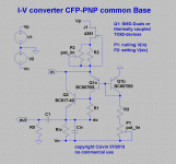
For the same conditions the simple CFP current conveyor sims far better.
It offers lower THD, lower noise, lower part number count/effort/cost and lower power consumption.
No difficulty in dialling into dc-bias and input-null points.
Merely a slight overshoot than tendency of oscillation.
Zin is higher but linear and low enough to not cause trouble with highimpedance output DACs.
JFET CCS provides for lowest noise of all CCS here.
Calvin , I have built a prototype of your CFP current converter, and it has a tendency to oscillate , but it gets stable with a 47pf cap between collector and base of Q2, the distortion is very low (0.0005%) -1db.
Shinja , the only good soluction that I have tested with a opamp I/V, and it sounds very good also, was using the capacitor of the "noise-gain compensation" as a filter for the noise generated by the DAC chip, This is something along the line of what Jcx is using.
I have to take a better look to what you propose , but not for now, I am very excited about the great performance and simplicity of the single-ended common base I/v , see post #22 , I discarded the jfet ccs and now I am using one with bc337, the noise is even lower. now the signal to noise ratio at 1 khz is better than 140db, the distortion is better than 0.0002%, I think is not easy to do it better") .
.
I have to take a better look to what you propose , but not for now, I am very excited about the great performance and simplicity of the single-ended common base I/v , see post #22 , I discarded the jfet ccs and now I am using one with bc337, the noise is even lower. now the signal to noise ratio at 1 khz is better than 140db, the distortion is better than 0.0002%, I think is not easy to do it better
.
Avro , that circuit don't work.
Edit: can you discover the error ?
I'm far from an expert...
I would guess that Q1 and Q2 forming a current
mirror won't work in that situation.
The top and bottom form a current sink and
a current source. They seem fine.
What's the error?
Hi,
Avro, compare Yout schem to the Jock as in #15. Think about the position of Riv/Civ and what that means to the DC-working point at the conveyor transistor´s collector
Sergio, I assume Your IV of #22 is a Jocko 2xNPN for conveyor and Ube-cancellation, 2xJFET-CCS.
I´m a bit surprised that the noise gets lower with the bipolars.
In my sims I used the 4391 for the lower CCS and that always gave lower noise than anyhing else, be it bipolar or more complex.
BTW: If one makes up the common Base (CFPed or not) with a PNP-conveyor and not an NPN as in #17, the CCS may run on lower current, thereby decreasing the required power.
Do You use the folded cascode as level translator to omit with a coupling cap?
jauu
Calvin
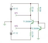
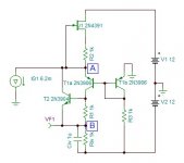
So I whipped up a simple sim for study.
With the values on the schematic, I get 9.8V
at VF1 and -119mV at VF2 as DC points.
R1 is the value that the DAC sees.
R2 sets the overall current through T1.
T2 turns T1 on.
R3 sets the current through T2.
Is that correct?
How do we choose the values for the resistors?
R3 only needs to put a couple mA through T2.
Assuming a PCM1794 in mono mode, how much current
do we need through T1?
What is a good value for R1?
Attachments
Hi,
As R2 (or a CCS) is of large impedance compared against the emitter impedance, the DAC will mainly see T1´s emitter impedance.
As R1 (or let´s call it Riv) is connected to T1´s collector (high-impedance norde), the transistor will see the Riv as load.
T1 is the current conveyor or as I like to name it the current buffer.
It presents the DAC a low impedance. This is what the DAC requires, since the voltage generated over this impedance by the DAC´s current must not exceed the DAC´s voltage compliance (allowed maximum voltage range), which is typically around +-1V.
T1, the current buffer, is not restricted to the low compliance voltage values, so it may work in impedance values sufficient to generate a couple of Volts.
If T1 and T2 are identical, the currents trough each need to be very similar.
Close, but not identical though, due to the differences in their respective Uce.
If T1 is a CFP, then the current through T1´s master is smaller, hence the current trough T2 may be smaller too.
Since the PCM is a current-sourcing DAC its current will have to be sinked fully.
The maximum the DAC can source is the 3.5mA centre current + 2mA peak signal current.
So, the current-sink must at least sink 5.5mA.
After Kirchhoff the current sum of all currents flowing into and out of a node equals 0.
Let´s assume now that the current-sink sinks 8mA. At idle the DAC sources 3.5mA. So 4.5mA must be supplied from T1´s emitter.
Not accounting for the small base current, the emitter current appears as the same as collector current and also flows trough R1.
The voltage drop over R1 defines the working point Vf1.
Now assume the DAC to source 5.5mA, its maximum current.
Then after Kirchhoff, T1s emitter will have to deliver 2.5mA. The current trough R1 will be 2.5mA.
The voltage drop will decrease, hence Vf1 will rise.
If the DAC supplies its minimum current of 1.5mA, T1s emitter will supply for 5.5mA, the voltage dropped over R1 increases, VF1 sinks.
It has probabely become clear by now, that the current through T1 must never be allowed to become 0.
Hence T1´s idle current must be greater as the DAC´s peak current, hence >2mA.
The voltage dropped over R1 is centered around Vf1=V2 - 3.5mA*R1.
The voltage swings with V~ = +-2mA*R1 around the centre value Vf1.
The values of R1 and V2 may be chosen after one´s specifications, but a good starting point for Vf1 is V2*0.5 as it´d allow for maximum voltage swing.
With 2mA peak DAC current (1.4142mArms) a R1 of 1k4-1k5 would result in app. 2Vrms voltage swing.
Say we choose R1=1k5, V2=12V supply and VF1 ~6V.
This would require idle current of 4mA flowing through T1 and 7.5mA through R2.
Vf1´s range would be from +3 to +9V, well within linear limits of T1.
With V1=-12V and Vf2~0V R2 calculates to 1k6.
Now choose T1/T2 a transistor with high and linear hfe over the required current range and low capacitances. For example the BC550, BC337, or the BC817, BC848BS in SMD.
The latter is especially well suited as it is a Dual, which increases thermal stability.
If You change to PNPs instead of the NPNs for T1/T2 (the complementary circuit), You will see that the DAC idle current runs trough T1.
If T1 is set to 4mA idle current again, R2 would only need to supply only for 0.5mA.
This reduces overall power consumption. Also the PNP is less noisy and has higher hfe. So output noise and input impedance at Vf2 will drop.
If a NJFET current source/sink is used for R2 it´s current setting resitsor will be larger, hence the source´s impedance will be higher.
Id-tolerances of the NJFET played a minor role with larger setting resistor too.
So going PNP for T1/T2 looks like an all-win situtation here.
Top of the cream will be a PNP-Dual with a single NPN as CFP-Transistor for T1 and a dedicated current source/sink for R2.
jauu
Calvin
No, the DAC will see the emitter of T1 and the paralleled resistor R2.R1 is the value that the DAC sees.
As R2 (or a CCS) is of large impedance compared against the emitter impedance, the DAC will mainly see T1´s emitter impedance.
As R1 (or let´s call it Riv) is connected to T1´s collector (high-impedance norde), the transistor will see the Riv as load.
T1 is the current conveyor or as I like to name it the current buffer.
It presents the DAC a low impedance. This is what the DAC requires, since the voltage generated over this impedance by the DAC´s current must not exceed the DAC´s voltage compliance (allowed maximum voltage range), which is typically around +-1V.
T1, the current buffer, is not restricted to the low compliance voltage values, so it may work in impedance values sufficient to generate a couple of Volts.
Yes, but R2 -or a current source instead- also takes over the DAC´s centre current (3.5mA with PCM1794).R2 sets the overall current through T1.
correct.T2 turns T1 on.
correct.R3 sets the current through T2.
R3 needs to be chosen such that T2´s Vbe is exactly T1´s Vbe.How do we choose the values for the resistors?
R3 only needs to put a couple mA through T2.
If T1 and T2 are identical, the currents trough each need to be very similar.
Close, but not identical though, due to the differences in their respective Uce.
If T1 is a CFP, then the current through T1´s master is smaller, hence the current trough T2 may be smaller too.
Assume R2 to be a constant current-source (well actually a sink here).Assuming a PCM1794 in mono mode, how much current
do we need through T1?
Since the PCM is a current-sourcing DAC its current will have to be sinked fully.
The maximum the DAC can source is the 3.5mA centre current + 2mA peak signal current.
So, the current-sink must at least sink 5.5mA.
After Kirchhoff the current sum of all currents flowing into and out of a node equals 0.
Let´s assume now that the current-sink sinks 8mA. At idle the DAC sources 3.5mA. So 4.5mA must be supplied from T1´s emitter.
Not accounting for the small base current, the emitter current appears as the same as collector current and also flows trough R1.
The voltage drop over R1 defines the working point Vf1.
Now assume the DAC to source 5.5mA, its maximum current.
Then after Kirchhoff, T1s emitter will have to deliver 2.5mA. The current trough R1 will be 2.5mA.
The voltage drop will decrease, hence Vf1 will rise.
If the DAC supplies its minimum current of 1.5mA, T1s emitter will supply for 5.5mA, the voltage dropped over R1 increases, VF1 sinks.
It has probabely become clear by now, that the current through T1 must never be allowed to become 0.
Hence T1´s idle current must be greater as the DAC´s peak current, hence >2mA.
The voltage dropped over R1 is centered around Vf1=V2 - 3.5mA*R1.
The voltage swings with V~ = +-2mA*R1 around the centre value Vf1.
The values of R1 and V2 may be chosen after one´s specifications, but a good starting point for Vf1 is V2*0.5 as it´d allow for maximum voltage swing.
With 2mA peak DAC current (1.4142mArms) a R1 of 1k4-1k5 would result in app. 2Vrms voltage swing.
Say we choose R1=1k5, V2=12V supply and VF1 ~6V.
This would require idle current of 4mA flowing through T1 and 7.5mA through R2.
Vf1´s range would be from +3 to +9V, well within linear limits of T1.
With V1=-12V and Vf2~0V R2 calculates to 1k6.
Now choose T1/T2 a transistor with high and linear hfe over the required current range and low capacitances. For example the BC550, BC337, or the BC817, BC848BS in SMD.
The latter is especially well suited as it is a Dual, which increases thermal stability.
If You change to PNPs instead of the NPNs for T1/T2 (the complementary circuit), You will see that the DAC idle current runs trough T1.
If T1 is set to 4mA idle current again, R2 would only need to supply only for 0.5mA.
This reduces overall power consumption. Also the PNP is less noisy and has higher hfe. So output noise and input impedance at Vf2 will drop.
If a NJFET current source/sink is used for R2 it´s current setting resitsor will be larger, hence the source´s impedance will be higher.
Id-tolerances of the NJFET played a minor role with larger setting resistor too.
So going PNP for T1/T2 looks like an all-win situtation here.
Top of the cream will be a PNP-Dual with a single NPN as CFP-Transistor for T1 and a dedicated current source/sink for R2.
jauu
Calvin
Last edited:
Sergio, I assume Your IV of #22 is a Jocko 2xNPN for conveyor and Ube-cancellation, 2xJFET-CCS.
I´m a bit surprised that the noise gets lower with the bipolars.
In my sims I used the 4391 for the lower CCS and that always gave lower noise than anyhing else, be it bipolar or more complex.
BTW: If one makes up the common Base (CFPed or not) with a PNP-conveyor and not an NPN as in #17, the CCS may run on lower current, thereby decreasing the required power.
Do You use the folded cascode as level translator to omit with a coupling cap?
Hi,
Calvin sorry for the delay on answer.
I never try the Jocko circuit , in theory the distortion will be worst than the simple common base because the upper ccs will contribute with added capacitance non linearity , but as I say I never try it.
I use relative high emitter degeneration resistor on the ccs to lower the noise, in #22 i use 440R , that is something that I learn with Joachim Gerhard.
I always use coupling cap, I prefer a polipropilene capacitor than using a integrator op amp, I think that a capacitor may influence in high power aplications like in loudspeakers , but not in low power like a DAC or a pré-amplifier , ofcourse a good film capacitor is mandatory.
I have made some I/V converters based on folded cascode in the past (and they do perform very well), but now I am testing various common base circuits.
I will post a simple common base jfet circuit soon.
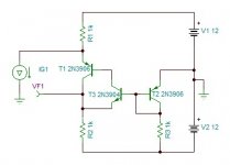
Hi,
more like this
jauu
Calvin
Thanks Calvin...I almost got it right...
So I got this entered into the simulator.
Now for some practical values.
I know we adjust R3 for minimum offset at "A".
We adjust R2 to set the value at "B".
What are some good starting values for
the Resistors? What operating points are
we looking for?
The PCM1794 has a center current of -6.2mA
and a peak to peak output of 7.8mA
Now for some practical values.
I know we adjust R3 for minimum offset at "A".
We adjust R2 to set the value at "B".
What are some good starting values for
the Resistors? What operating points are
we looking for?
The PCM1794 has a center current of -6.2mA
and a peak to peak output of 7.8mA
Attachments
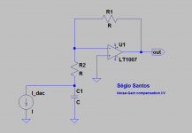
op amp iv i/v voltage output
Hi,i see this circuit everywhere,but whats the formula to calculate the output voltage?
Why pupdac has 220R to gnd,because it will change the meaning of the circuit from i/v to a `voltage cutter,
noise-gain compensation I/V.
is better to use a decompensated opamp, but I have try with the opa2134 and it works very good, the best sound of all the opamp based I/V converters I have listening.
Hi,i see this circuit everywhere,but whats the formula to calculate the output voltage?
Why pupdac has 220R to gnd,because it will change the meaning of the circuit from i/v to a `voltage cutter,
Hi,
as transistors I´d choose:
- T1: Duals for thermal tracking, low voltage, low capacitance and linear and high hfe over the desired current range.
SMDs like Dual BC557 or Dual BC807 will suffice, since the current through them will be small --> hence low heat power loss.
Idle currents around 0.5-1mA will be fine. choose 1mA
- T2: will have to take the ´rest´ of the dac current + the idle current of the JFET-CCS. Which is roughly +-3.9mA +5.2mA + Ijfet. BC550, ZTX 750, 790 may suffice or SMD equivalents like BC817, 850, FZT651.
- J1: a high Vgs, high Idss, lownoise, low capacitance JFET in TH or SMD like the 4391 will suffice. Since the idle current through J1 remains low, SMD casing will suffice power loss wise.
As the DACs idle current settles at 6.2mA a 1k Riv resistor would give an voltage drop of 6.2V, and result in a DC-bias voltage of -5.8V with 12V supplies, which is already too much.
3.9mA current amplitude means 3.9Vpeak or 2.76Vrms.
2Vrms will be more than enough to drive almost any amplifier into saturation, so lets reduce the signal swing to 2Vrms -->2.83Vpeak.
This requires a Riv of 707R. Choose standard value of 750R.
6.2mAx750R=4.65V drop over Riv at idle, or -7,35V DC-Bias with -12V supply rail.
Choose DC-bias roughly half the supply rail, between -6.5V and -7V (to account for the Vbe drops of Q1a and Q2)
This means another 0.5mA to 1.1mA that J1 needs to supply for, to drop the additional 0.35V to 0.85V over Riv.
R1 controls the distribution of currents through Q1a and Q2. With rising value more current is directed through R2 and less through Q1a. R1 also affects THD. Lower currents through Q1a tendentially improve on the THD-figures.
Start with 500R and adjust for IQ1a between 500µA and 1mA.
Now Q1b needs to be tuned to equal Vbe like and Q1a. Start with Q1a´s idle current of say 1mA. The values are not exactly he same, since Q1a´s collector settles at Vdcbias-Vbe(Q2), so somewhere around -6.9 to -5.9V, while Q1b´s collector sits at Vbe(Q1b), ~-600mV. So 11.4V need to be dropped over R3. R3=11.4V/1mA=11.4k. choose R3 a series connection of 10k + 5k pot, or a parallel of 15k and 100k pot (I prefer the parallel connection, as it keeps the circuit functional in case of a pot failure like contact loss of the wiper. Btw, the same applies to the source resistor of J1).
R2, J1´s source resistor certainly needs trimming with off of the shelf JFETs.
4k7 to 5k paralleled with a 20k pot should be a good start here.
In case of oscillation a small cap (10-100p) or RC (100R/100p) from Q2´s emitter to its base may stop oscillation and clean-up square wave behaviour.
The voltage over Riv needs to be dc-coupled to the next stage. 10µF, working into a 100k grounded pre-load resistor will suffice.
jauu
Calvin
Last edited:
Hi all,
after a long read through a lot of pages about I/U converters (needed 3 days), i`m interested in building the CFP I/U converter discriped by Calvin.
I want to implement it in a Yamaha CDS1000.
I have a lot of BC337 and BC327 from the Paradise group buy and like to know if they would work in the cirrcuit.
As CCS i may use BF245 or BSS129 or 2sk170.
Maybe some of the more experienced DIY members have a suggestion on it.
If somebody can sim it, it would be fantastic.
The Yamaha uses PCM1796 in Monomode, so i have two differential outputs for left and right.
I´m confused how to connect the I/U converter to the PCM1796.
I want to use a symmetric analog output.
Version 1:
i connect first negative i out to input of the CFP I/U and the positive i out to PCM ground
second neg i out to PCM ground and positive i out to a second CFP I/U unit
and CFP I/U ground to PCM ground
Version 2:
like version 1 but first positive i out and second negative i out connected to each other and not to ground ( i outputs in series)
Version 3: both i outputs in parallel
If i think right Version 2 means higher output impedance and should be prefered.
Version 3 means more current and lower output impedance.More current is not necessary and lower impedance means worse distortion figures.
But what is about Version 1??
The differences maybe in the signal current loops.
I don`t know because after 3 days of reading my brain is boiling.
And i`m not a elctric engineer.
I hope you can help me to hit the Yamaha in the back, because it sounds ugly compared to other players i have heard.
Thanks and greetings from Germany
Roland
I
- Status
- This old topic is closed. If you want to reopen this topic, contact a moderator using the "Report Post" button.
- Home
- Source & Line
- Digital Line Level
- Current differential to voltage line level from PCM1794 et al