Can I pull the pcb out of my Marantz cd-65 and make a DAC?
I was thinking that no matter what the chinese can throw at me I would still get a better PCB if I were to remove the Marantz CD-65 Standard Phillips tda1541 mainboard out of the player and put it into my own custom case for the purposes of a DAC.
I was thinking of just plugging an I2S bus into the TDA1541's pins and seeing if it worked or not.
The cd transport is almost completely shot mechanically so theres no point in saving that.
What does the SAA7220 do in relation to the TDA1541?
What else can I pull or chip away without affecting the DAC? Obviously the beautiful flourescent display can get the boot, a recapping of the power supply is in order, aside from that?
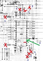
Is that additional floating board a reclock circuit? Should I toss that and plug the 8441P right into the mainboard?
Here are some pics so you guys can get an idea of the job at hand.


I was thinking that no matter what the chinese can throw at me I would still get a better PCB if I were to remove the Marantz CD-65 Standard Phillips tda1541 mainboard out of the player and put it into my own custom case for the purposes of a DAC.
I was thinking of just plugging an I2S bus into the TDA1541's pins and seeing if it worked or not.
The cd transport is almost completely shot mechanically so theres no point in saving that.
What does the SAA7220 do in relation to the TDA1541?
What else can I pull or chip away without affecting the DAC? Obviously the beautiful flourescent display can get the boot, a recapping of the power supply is in order, aside from that?
Is that additional floating board a reclock circuit? Should I toss that and plug the 8441P right into the mainboard?
Here are some pics so you guys can get an idea of the job at hand.
Last edited:
no, you cannot give the SA the boot, it is everything, without it, or some custom digital filter, your dac is useless. feeding i2s to the TDA will make a raucous noise if anything at all. the SA is the digital filter.
some of the old CD players with TDA were very high quality, this does noit appear to be one of those times.... the voltage compliance and clocking will be all wrong for a dac I would think too, so this may not be as simple, or cheap as you presume.
better to just pull the DAC chip and use in one of the many designs on this forum and others
1541 takes the i2s for breakfest. 7220 too, so you can choose between NOS/OS (OS for me is better) by bypassing the DF.
Clocking et cetera... cut the traces, shut everything down but the 7220, 1541, and the analog stage. Make sure you have disabled the deemphasis filter there.
Keep the PS, add some SPDIF receiver with 256mclk and you're done. Just configure it into some acceptable by 7220 i2s format.
Clocking et cetera... cut the traces, shut everything down but the 7220, 1541, and the analog stage. Make sure you have disabled the deemphasis filter there.
Keep the PS, add some SPDIF receiver with 256mclk and you're done. Just configure it into some acceptable by 7220 i2s format.
Hi,
That floating board is a 'Fix' by Philips for the control circuitry, some later players had a single chip in there.
I notice that this is non A TDA1541 chip - Qusp, is this different to the A? With the A you can get rid of the filter, I need to revisit the datasheets but IIRC the non A version also needs a system clock input on pin 4.
I have done exactly what you describe but I replaced the TDA with the 'A' version, I then built a PSU for the DAC and a separate output stage, I then supplied the i2s signal from a PCM2706 USB decoder straight to the DAC - works perfectly!
If I get a bit of time I'll take some photos and sketch up the schematics from the service manual.
Cheers
Josh
no, maybe i'm mistaken, it could be that i'm simply used to seeing a good many TDA1541A dacs that need specialized black magic clocking circuits to gain good performance out of this dac, with synchronous 4x OS DEM reclocking etc; so figured a digital filter or equivalent flip-flop/logic circuit was needed.
Secondary to this and part of the reason for my answer, is what clock speeds are available/in use on the board? I wouldnt expect good performance from just plugging in an external i2s source and using its matching MCLK if available. we can presume it accepts PCM since it worked with your PCM2706? which flavor of i2s specifically are we talking about here that is accepted natively left justified, right justified, PCM, i2s etc? did you supply a masterclock to go with the i2s? because MCLK is not part of the i2s standard. what settings are/could be hardwired into this PCB with pull-up/down resistors?
but i'll let someone who knows this dac answer more specifically, as I would need to look up its datasheet to make more reliable commentary. of course the SA7220 does take i2s, but from what I have read it tends to crap noise all over the power supply rails, so needs careful attention to decoupling
Last edited:
my I2S source is a CS8412, hardwired to a piece of perfboard:
I decided to scrap my TDA1543 DAC, I ended up not liking the sound of it and greatly preferred the sound of the TDA1541 that is in this CD player.
This board has two 7805 vregs onboard dedicated to the CS8412's digital and analog lines, but have the same copper earth bus.
What I can do is plumb the I2S out of this board into the SAA7220 or the TDA1541 chip and cut back some traces as another poster here has said.
Or failing that I can pull the TDA1541's socket and soldering it to this perfboard and going from there, I have found a few schematics which might be suitable:
http://www.fetaudio.com/wp-content/uploads/2009/10/TDA1541.pdf
http://2.bp.blogspot.com/_u_EoD7hGI...a9c/s1600-h/TDA1541+schematics+Duka+Rev+2.gif
But nothing completely certian, I don't want to end up losing this TDA1541 chip to the smoke ghosts as I'm actually very fond of its sound but I've run out of CD material to feed it with, hence the need/desire and want to keep it all on the original phillips reference board.
If I cant then Im going to pull the transformer and voltage regulators and rebuild the entire thing on a new board, I'm hunting for a scrap transformer at the moment so I don't have to do that.
Last edited:
I suggest just chucking the PCB and doing it properly. now there is of course John Brown's Epic thread on the development of his dac with TDA, very good, but very involved. you will be able to get up and going with this brief, but complete and well constructed post by Thorsten Loesch, who is a well known professional designer of the CD77. I tend to feel his approach is better anyway.
what you have above there looks like a good way to make an RF antenna, Thorstens attention to detail in grounding with solid copper foil layers is very good and accessible DIY construction, as well as excellent instruction on power supply and decoupling. if you dont have any copper foil, I could send you enough for this board in an envelope.
what you have above there looks like a good way to make an RF antenna, Thorstens attention to detail in grounding with solid copper foil layers is very good and accessible DIY construction, as well as excellent instruction on power supply and decoupling. if you dont have any copper foil, I could send you enough for this board in an envelope.
I suggest just chucking the PCB and doing it properly. now there is of course John Brown's Epic thread on the development of his dac with TDA, very good, but very involved. you will be able to get up and going with this brief, but complete and well constructed post by Thorsten Loesch, who is a well known professional designer of the CD77. I tend to feel his approach is better anyway.
what you have above there looks like a good way to make an RF antenna, Thorstens attention to detail in grounding with solid copper foil layers is very good and accessible DIY construction, as well as excellent instruction on power supply and decoupling. if you dont have any copper foil, I could send you enough for this board in an envelope.
Thanks for the help guys, and merry christmas.
I have a brand new roll of adhesive copper foil actually but thanks for the offer, the difficult part is understanding how to lay it down so it can trap that digital noise and earth it.
I have plenty of large perfboard and a solder sucker, so I can always start again. I also havent overheated the IC, been using a 30 watt iron and doing the bare minimum heating time with standard flux core solder.
I was thinking of laying down some copper tape underneath the IC, then doubling that ontop of the IC, earthing both strips at one end, the 14th pin end, then getting some copper tape and making a trap around the pcb board to surround it with copper tape, like a box with a capital I in the center, the I representing the copper that goes underneath and above the CS8412.
Last edited:
These are the snips to the PCB for supplying a dedicated PSU and i2s. I didn't supply a separate clock - I have one but haven't got round to implementing it yet!
I get pretty good results just from the 2706 (this is all relative though! ie it's a big step up from the original CDP but for all I know could be miles away from a properly implemented dac). I'm a great believer in getting it working first then tweaking it!
From the datasheet you can see that with pin 27 connected to +5v (as in this case) the input format is accepted as Time MUX (2's complement).
I just took the Bit Clock, WS, Data & Ground straight from the 2706. I too have seen some very elaborate clocking schemes and will try to get round to implementing a few when I get chance.
On the diagram then;
1 - -15v Supply
2 - +5v Supply
3 - LE/WS Input
4 - BCK Input
5 - Data input
6 - -5v Supply
7 - Left Channel Output
8 - Right Channel Output
9 - On the TDA1541 datasheet it states that you need to supply a System Clock to pin 4 for NOS operation, on the A version you can leave this open. If you need to supply system clock then cut the trace indicated by the red line - however there's no easy way to attach a cable, you could solder straight onto the chip leg but be careful!
As mentioned earlier - all my work was done with the same PCB but I had replaced the DAC chip with the A version - I can't confirm that this will work with the non-A chip on your board!
I do have a non-A version so I might try it!
Cheers
Attachments
no problem, indeed 


 take your pick
good luck with the TDA1541A, seems it turns into a loooooong journey for most but the above link cuts to the chase pretty quickly, hes got a matching tube stage posted around somewhere too, if you like Glass
honestly I dont think those 2706 are worth the effort, very high jitter by todays standards, there are many better options available here on the forum. if it accepts i2s and PCM, then just grab one of the DSD and i2s/PCM convertors like the Amanero combo384, which with the number sold in the DIYAUDIO GB means its like 39EU for our GB, which is ongoing at that price for us. you will find the latest google groups GB page linked in that thread somewhere, make sure to get the latest link because i'm not sure he fixed the first link when he moved it.
it does DSD over USB with the right dac, as well as 44.1-384kHz PCM. It is a minimal but fairly well thought out module with easy external power and isolation if you like, the onboard regs are very low noise LDOs, so not a bad start. you can tap the master clock (it has dedicated clocks for 44.1x and 48x for the audio as well as its own clock) plus there are some mods for isolated and reclocked output. which will allow tapping a proper master clock
the device is this one here
take your pick good luck with the TDA1541A, seems it turns into a loooooong journey for most
but the above link cuts to the chase pretty quickly, hes got a matching tube stage posted around somewhere too, if you like Glasshonestly I dont think those 2706 are worth the effort, very high jitter by todays standards, there are many better options available here on the forum. if it accepts i2s and PCM, then just grab one of the DSD and i2s/PCM convertors like the Amanero combo384, which with the number sold in the DIYAUDIO GB means its like 39EU for our GB, which is ongoing at that price for us. you will find the latest google groups GB page linked in that thread somewhere, make sure to get the latest link because i'm not sure he fixed the first link when he moved it.
it does DSD over USB with the right dac, as well as 44.1-384kHz PCM. It is a minimal but fairly well thought out module with easy external power and isolation if you like, the onboard regs are very low noise LDOs, so not a bad start. you can tap the master clock (it has dedicated clocks for 44.1x and 48x for the audio as well as its own clock) plus there are some mods for isolated and reclocked output. which will allow tapping a proper master clock
the device is this one here
Last edited:
thanks for getting back to me, I think I'll wait for you to do that test if thats alright with you to do it, that would simplify things a great deal.
The problem with the red baron is that its like half my income for a month gone just on some PCB's, and all for a lowly old TDA1541 non-A? sheesh..
I understand what youve done there in the schematic, I would leave the psu's in place for now tho.
It is my understanding that the CS8412 pin 11 FSYNC output goes to pin 4 DATA R/SCK input on the TDA1541 according to this schematic:
http://www.fetaudio.com/wp-content/uploads/2009/10/TDA1541.pdf
Shouldnt be too difficult to put a 74HC4050 in-line should it.
Last edited:
fast logic chips for audio signals is one of the hardest things to get right for PCB layout actually
ah....
ah....
because it and its power supply demands comes directly from the RF layout manual, used for digital, but with a very analogue purpose, mixed signal design at its best, nothing that comes from one school of thought only will come up with the goods.
fast logic chips for audio signals is one of the hardest things to get right for PCB layout actually.
also Thorsten gives that Red Barron a worse review than the Ebay dacs in that thread I linked and he doesnt think kindly of those....
almost missed that, yes, it looks to me like someone has spent too much time in pcb cad software, especially the first pcb design.
I was reading up on thorstens comments earlier... mmm
I bet if I put the tda down onto some perfboard and point to point wire everything analog and pcb wire everything digital and then create little copper shield boxes for the digital pcb that maybe i could make a nice sounding dac.
Something to think about anyway.
That pin 4's a bit odd, according to the 1541A datasheet it can be left unconnected but in most designs you see see it connected to pin 2.
On the 1541 datasheet it says to connect it to the system clock.
That said, in the player I have (same PCB as yours) with the original 1541 you can see that it's connected to pin 2 as per the A. I tried it both ways on the A and couldn't tell any difference!
There's also the question of the DEM cap, on the 1541 datasheet pins 17 & 18 are not connected but on our players we have a cap accross them as per the A version!! This cap makes a big difference on the A but the non-A? who knows?
It might be a few days before I get a chance to try the non-A in this config but I'll keep you posted!
Leaving the PSU's in place is fine if you're bypassing the 7210 & 20 as they're noisy, if you leave them in place then it's worth providing a clean +5v to the 7220, just an LM317 is ok - all the better if it's got it's own traffo.
The only issue I can see with the perfboard is the decoupling caps as they're close together - they're smd on our pcb's so it's not an issue, on perfboard you could go half on top, half underneath to keep them close to the dac?
Qusp - I'll have a look at that USB decoder thanks! I need to move on from the 2706, it was lying around from an old project so when the mech in the cdp packed up it was handy.
Have a great Christmas!
I'll have to figure something out anyway, I've got insomnia again so I won't even be ready until tomorrow at least to start experimenting.
It certianly sounds exciting I know that much, I'm leaning towards leaving it all in the phillips pcb because I don't feel like making a new I/V stage at the moment, which means either giving the SAA7220 a signal or cutting it out of the loop.
I doubt the CS8412 will go high enough to get to 174.4KHz, 24bit.
Hi Freax,
If your ok with etching PCBs, then you may just as easily make your own board for the 1541.
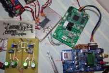
Here is my current setup with the TDA1541A, sounding great but still just a prototype. I will change the current grounding layout of the DAC and also integrate the CEN on the same board for the next version.
Ryan
If your ok with etching PCBs, then you may just as easily make your own board for the 1541.
Here is my current setup with the TDA1541A, sounding great but still just a prototype. I will change the current grounding layout of the DAC and also integrate the CEN on the same board for the next version.
Ryan
Attachments
[EDIT] I think I have WS and BCK around the wrong way! lol, I'll check it and try again.
This is what I've come up with so far, there is only 3 wires connecting to the TDA's pins, LE/WS aka SCK and BCK aka FSYNC, and the third, SDATA aka DATA L and DATA R.
I don't have much experience with this so I'm working in the blind here, the CS8412 is producing a signal as I've verified it with my TDA1543 dac.
I lifted the old bridge wires and connected my own wires with the cable coming from the TDA1543 dac.
However it doesn't work, do I need to connect a ground lead aswell? I'm about to do that, then after that I'm going to lift that trace connecting pins 2 and 4 and give it a clock signal from the CS8412
Last edited:
[EDIT] I think I have WS and BCK around the wrong way! lol, I'll check it and try again.
This is what I've come up with so far, there is only 3 wires connecting to the TDA's pins, LE/WS aka SCK and BCK aka FSYNC, and the third, SDATA aka DATA L and DATA R.
I don't have much experience with this so I'm working in the blind here, the CS8412 is producing a signal as I've verified it with my TDA1543 dac.
I lifted the old bridge wires and connected my own wires with the cable coming from the TDA1543 dac.
However it doesn't work, do I need to connect a ground lead aswell? I'm about to do that, then after that I'm going to lift that trace connecting pins 2 and 4 and give it a clock signal from the CS8412
Best way with ribbon cable is - GND-BCK-GND-WS-GND-DATA-GND
This way return current will be close to signal to ensure lowest impedance (for ribbon cable). A better choice is mini coax (U.FL for example).
- Status
- This old topic is closed. If you want to reopen this topic, contact a moderator using the "Report Post" button.
- Home
- Source & Line
- Digital Line Level
- I don't feel like giving the chinese more money, can I pull the pcb out of my cd-65?