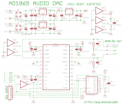
I presume the 24 pin device is the AD1865, if so you may want to check the Iout pins 4 and 21 they seem to be connected directly to GND, also the SJ pins.
The resistor and caps hanging off these lines also do not connect to anything apart from each other.
Is it based on the schematcis in post 4 or 5?
The resistor and caps hanging off these lines also do not connect to anything apart from each other.
Is it based on the schematcis in post 4 or 5?
Last edited:
Yes the big IC is AD1865. Im using the Iout schematic for both 24 bit and 24bit/192khz boards (24bit/192 khz is Vout on pavouks site).
I think i messed up the I/V resistor and cap connection, right? They should have a connection to ground
I think i messed up the I/V resistor and cap connection, right? They should have a connection to ground
Attachments
Last edited:
 Thanks marce for pointing this out
Glad to help, I spend all day looking at schematics, data sheets and PCB's, luckily the system I use the schematic and PCB parts are interlinked so I don't get these problems (Cadstar).
A good tip is to get some coloured highlighter pens and trace over the lines with yellow when manually transferring, green for the first check and red for the final check.
A good tip is to get some coloured highlighter pens and trace over the lines with yellow when manually transferring, green for the first check and red for the final check.
Last edited:
O yesHow about a dual AD1865 with I2S input and I-out board?")
O yes
Those extra 6 bits added with the logic chips proably aren't adding resolution, it was more of a marketing gimmick that one manufacturer came up with in the 90's, I would want dual mono with LSB adjust to get the most out of this chip.
I've been dreaming about a dual AD1865 with I2S and balanced tube stage for a while but still nothing comes true. The only thing I came up with is this Matej's audio pages: Dual balanced NOS DAC AD1865 board but the author seemed to lost interest right after posting the layout... SPDIF is just the past to me right now.
Just a small board with headers for external modules (PSU, USB-I2S, IV) would be perfect. Heck, I will even offer free board as a gratitude for anyone comes up with this design.
Just a small board with headers for external modules (PSU, USB-I2S, IV) would be perfect. Heck, I will even offer free board as a gratitude for anyone comes up with this design.
Last edited:
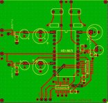
I made a few changes: Made the tracks a bit thicker (0.64mm) fixed a connection to pin 14 of AD1865 that didnt exist, moved the regulator closer to analog +5v supply of the IC and also made a board without Mic5207 regs for experimentation purposes. I will probably etch and build the boards on monday hoping that alligning the toner transfers wont be a huge pain(also hoping that the boards actually work! ).
).Attachments
I run into a problem today. I soldered all regulators and went ahead with testing their voltages. The regs for positive supply all work ok, giving V+ 4.97-4.98V.
The regulator for the negative supply is measuring V+ 0.6v and gets very hot to touch. (By the way, the pictures i posted show the negative supply reg wired wrong)
I am using two seperate transformers to feed the regs with the ground pin of the negative supply reg as V-, and the Vout pin connected to ground plane.Am i overlooking something?
Edit: All regulators are positive
I think you need a proper negative regulator.
Tried two mic5207's and a 78l05. The same result, all get very hot and give 0.6v+ . Im going to buy a 79l05 tomorrow to give it a try hoping it works. Im still puzzled though why is this happening
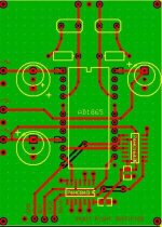
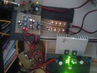
Using an 79l05 reg the dac works perfectly. Wired it today and sounds really good although using such a noisy reg for negative supply.Now i have to find a low noise negative reg with high-ish input voltage.I changed the layout of the board to reduce the number of slots in the ground plane. Picture quality is bad and the dac is a mess in its current form (long wires, uncut boards ,etc)
Attachments
Getting well Skouliki, great !
Question to the clocking and IV experts :
- If I was to connect 3 of these DACs to I2S out of Najda Digital XO, should I do something to synchronize properly the 3 DACs/avoid jitter (eg share the same clock ...)
- What is the best IV for these boards ? Zen/Cen/Sen ? (I have tube SRPP on my Raindrop board that work great, I could also duplicate them)
BR
Jean-Louis
- Status
- This old topic is closed. If you want to reopen this topic, contact a moderator using the "Report Post" button.
- Home
- Source & Line
- Digital Line Level
- AD1865 schematic