Please allow me to advise.
This board Ian is making will allow the option of a simultaneous output of offset binary Left and Right Data. For TDA1541 enthusiasts, and tinkerers, this will allow a person to create a dual mono TDA1541 board. Also possible is a dual differential, or balanced output TDA1541 board.
I know many people will be interested in these possibilities.
And it may be worth nothing, but I have read reports from those that have tried it, that the offset binary data input sounds better than the i2s.
I don't know, but I am keen to try it.
It will also allow the use of the TDA1540 chip.
In seeing pictures of PCM board, the connections (single TDA1541) would be as follows?:
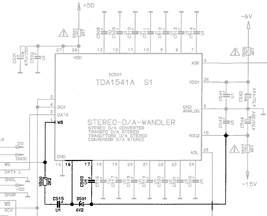
LLLR to Pin 1 (LE/WS)
CLK to Pin 2 (BCK)
DL to Pin 3 (Data L)
DR to Pin 4 (Data R)
-5V to Pin 27
This would result in balanced output?...or did I misunderstand?
can a synchronous oversampled 4-8*FS output from this board be fed directly to the TDA for DEM reclocking, or is the only way to adjust the DEM by the use of specific capacitor values to adjust the normally free-running clock?
You need to divide the oversampled output by 2 or 4 respectively if you want to try DEM reclocking with oversampling.
Adjusting the capacitor value between pins 16 and 17 is another way to adjust the speed of the free running clock- but in which case it will not be synchronized. My 2c is that the Grundig method is the best sounding reclocking method. here I made some comments about the sound.
In seeing pictures of PCM board, the connections (single TDA1541) would be as follows?:
LLLR to Pin 1 (LE/WS)
CLK to Pin 2 (BCK)
DL to Pin 3 (Data L)
DR to Pin 4 (Data R)
-5V to Pin 27
This would result in balanced output?...or did I misunderstand?
How you said will output stereo data.
For a single balanced channel you would have to for example, apply DL to (data L) and use an inverter to apply /DL to (data R) this will make a single chip with balanced output.
....And now you have me thinking if you need to invert the MSB on the inverted data as well. Does anyone else remember? The last time I inverted a binary number was at school and the part I needed to remember to answer this question leaked out my ear in my sleep...

Last edited:
For a single balanced channel you have to invert data and add one....For a single balanced channel you would have to for example, apply DL to (data L) and use an inverter to apply /DL to (data R) this will make a single chip with balanced output...
Ian, since the board has physical support for inverted data lines is it possible to squeeze balanced mode into the CPLD (add one to the inverted data lines)? As J2 header has some unused pins this feature could be optional.
Thanks, Zsolt
Last edited:
interesting, thanks for the replies guys, completely for curiosity, I dont plan to try it out but I do find the TDA internal architecture quite interesting all the same. i'm a complete no nothing when it comes to the 1541A. if I was to grab this board though it would mainly be for playing with a possible 1704 dac, OR toying with discrete ladders and even custom programmed FPGA based dac array clocking.
For a single balanced channel you have to invert data and add one.
Ian, since the board has physical support for inverted data lines is it possible to squeeze balanced mode into the CPLD (add one to the inverted data lines)? As J2 header has some unused pins this feature could be optional.
Thanks, Zsolt
Hi Zsolt,
Yes it is possible. As you found, J2 reserved exactly for those purpose.
Regards,
Ian
For a single balanced channel you have to invert data and add one.
Ian, since the board has physical support for inverted data lines is it possible to squeeze balanced mode into the CPLD (add one to the inverted data lines)? As J2 header has some unused pins this feature could be optional.
Thanks, Zsolt
Thanks, I knew there was a trick to it
Last edited:
Hi Zsolt,
Yes it is possible. As you found, J2 reserved exactly for those purpose.
Regards,
Ian
Great!
For a single balanced channel you have to invert data and add one.
Having looked again at offset binary, I think it would not matter if we don't add the one.
It would probably add more jitter trying to add the one........
Last edited:
Qusp, the 1541 has limited bandwidth to about 6.5Mhz. The DEM has successfully been clocked from BCK at 2.8Mhz by several members following such designs as member "ecdesigns" (John Brown) has used in the past.
ecdesigns keeps changing his mind as to what sounds "better". He used to reclock his DEM really fast. Last I read he had gone to a slow, free running clock using a big capacitor between pins 16 and 17.
ecdesigns keeps changing his mind as to what sounds "better". He used to reclock his DEM really fast. Last I read he had gone to a slow, free running clock using a big capacitor between pins 16 and 17.
Yes i know, its a little confusing, but his willingness to experiment and be creative is always good to read about in his thread. At least it sparks some type of discussion.
I'm currently trying to determine what DEM frequency sounds best. I've currently got it running at 88khz.
My understanding of his latest reasoning is that the lower the DEM, the less crosstalk and resulting jitter imposed upon BCK to trigger the latch enable.
sorry, a bit off topic...
Hi new2hifi,
Since the TDA1541A accepts the I2S format directly, there is no point converting from I2S to PCM if you want to run the 1541 in NOS.........
Ryan
Thanks for information regarding TDA1541A ryanj. But original question is still unanswered.
Does this I2S to PCM convertor board oversample everything? If yes, then oversampling is a forced operation or optional?
Last edited:
Thanks for information regarding TDA1541A ryanj. But original question is still unanswered.
Does this I2S to PCM convertor board oversample everything? If yes, then oversampling is a forced operation or optional?
new2hifi,
My understanding is that no oversampling is done by the use of this board. This board is used to change data format.
Thanks for information regarding TDA1541A ryanj. But original question is still unanswered.
Does this I2S to PCM convertor board oversample everything? If yes, then oversampling is a forced operation or optional?
It could only be used for interpolation to 8X no filtering so technically not oversampling. Its really just format conversion for NOS, or if you want to oversample you could do that with your computer. I don't think it is worth asking iam for 8x interpolation as it isn't useful for anything.
For average NOS single chip TDA1541A build you wouldn't need this daughter board since the TDA1541 accepts 64fs blck i2S.
But for the high end NOS tda1541A it would be usefull for dual differential simultaneous mode using the offset binary. Some really fantastic measurements have been shown that dual differential TDA1541A helps cancel some of the TDA1541's tendancy to have extra 2H (see Tazz's threads.) Using thing daughter board rather than discrete work-arounds could prove very useful, ie. it really helps with the output stage. Dual differential mode done right (potentially with this daughter board) also takes you closer to an S2 grade tda1541 as far as measurements go.
The more I think about it I think we will all be crying for a dual differential simultanious offset binary mode for the TDA1541A, so might want to include it now.
TOTAL = 53
TV Man x 2
merlin el mago
rtd
jameshillj
erin
Nikola Krivorov x 3
Rupor54
vitalica
analog_sa
andrea_mori x 5
dsavitsk
tagheuer
hirez69 x 2
ccliu
BDL
cddumat
regal
zoran
Jogi
Zen(zenelectro) x 2
Buzzforb
SPWON
crobbins5421 X 2
marcus1 X 2
casshan x 2
Dweeb99 X 2
jackw X 2
kazap X 2
danzup x 3
Giordano x2
Tony_T
Tubo x1
clivem x2
noizas x2
- Home
- Source & Line
- Digital Line Level
- Drive NOS AD1865/62,PCM1704/02/63,TDA1541 from FIFO: Universal I2S-PCM driver board