I've been down this road before, and thought about it a great deal. This take on the matter from the link above pretty much sums up what I agree with
Calculations for PWB Trace Termination and Reflection values
"Source Termination may effect the rise time of the signal because of the RC time constant [R of resistor, C of the cable]. The driver is specified with a rise time based on some unit load [say 10pF], the rise time will be reduce to the R * C time constant with the series resistor. As the rise time is decreased the over all current demand from the driving pin is also reduced. Reducing the rise time has one benefit, reducing the Instantaneous current demand on the driver [reducing ground bounce and EMI] A series terminated line does not stop reflections [the load is still not terminated, un-matched], but it does reduce [damp] the amplitude of the ringing."
With digital audio, especially at the mixed signal device (DAC chip) you need to do all possible to avoid digital contamination of the analog output. The chip die wire connections to pins are very close, so you want to reduce coupling effects from pin to pin. And the effects of ground bounce from fast transitions can also create DAC conversion problems.
In my opinion, you need to examine which clock and data lines need sharp transitions (those that effect data conversion timing, i.e. jitter) and which don't. By fast transitions, I'm referring to fast rise and fall times.
In general, my experience is you should load the data frames reliably, but use the slowest transition time possible to get the job done. This approach also requires you to research what clock reference the DAC chip uses to control/trigger the conversion timing - it's either the L/R clock or bit clock. That one needs to be fast, (but not ringing) the others should be as slow (longer rise and fall times) as possible, to still work.
This edge speed is controlled by the value of the series resistors.
This is not a textbook approach, it's what works for me in this particular application. You need a decent scope (2GS/s or faster, 500MHz) and decent probes (500MHz active or better) to really observe what's going on.
The main skill in designing PCB's is component placement, the success of the design depends on good comp placement, the rest should then follow. Autorouters, very very rarely use them, may use them interactively for little areas and to get a metric on placement but that is it.
Some analogue digital design links, mainly relating to ground and how to placethe components...
http://www.hottconsultants.com/pdf_files/june2001pcd_mixedsignal.pdf
AES 2006 ? Henry Ott, Saturday - Anablog | Blog on EDN
http://www.hottconsultants.com/pdf_files/aes-2007.pdf
http://www.elmac.co.uk/pdfs/Lord_of_the_board.pdf
An intuitive, practical approach to mixed-signal grounding
http://focus.ti.com/lit/an/sbaa052/sbaa052.pdf
http://focus.ti.com/lit/ml/slyp167/slyp167.pdf
http://www.ieee.org.uk/docs/emc1206a.pdf
http://www.icd.com.au/articles/Split...s_AN2010_6.pdf
http://www.analog.com/static/importe...0Grounding.pdf
http://www.analog.com/static/importe...als/MT-031.pdf
Common Mode Ground Currents
PCB Stack-Up - Part 6
Tech Tips
Analog Devices: Analog Dialogue: Ask The Applications Engineer - 12
http://www.ti.com/lit/ml/slyp167/slyp167.pdf
Twisted pair cables
And some general info on PCB design, the misc section has a couple of tutorials...
http://www.elmac.co.uk/pdfs/Lord_of_the_board.pdf
IEC 60950 Glossary
Star Grounding Wars
http://www.cvel.clemson.edu/Presentation_Slides/PowerBus-Decoupling.pdf
PCB007 Quiet Power: Resonances in Power Planes
PCB007 Quiet Power: How Thin Laminates Suppress Resonances
PCB007 Do Not Perforate Planes Unnecessarily
http://www.ipblox.com/pubs/DesignCon_2011/11-TA3Paper_Weir_color.pdf
http://electrical-integrity.com/Quietpower_files/Quietpower-6.pdf
http://electrical-integrity.com/Quietpower_files/Quietpower-7.pdf
http://electrical-integrity.com/Quietpower_files/Quietpower-8.pdf
http://electrical-integrity.com/Quietpower_files/Quietpower-9.pdf
http://www.electrical-integrity.com/Paper_download_files/EPEP98_DET.pdf
Ground Pours: To Pour or Not to Pour?
http://www.goldphoenixpcb.biz/pdf/Loop_Area_Decoupling.pdf
beTheSignal - BTS-305 Battling Ferrite Superstition
http://www.speedingedge.com/PDF-Files/BTS006_What_Is_Inductance (2).pdf
MIL-STD-461: Requirements for the Control of Electromagnetic Interference Characteristics of Subsystems and Equipment - Advanced Test Equipment Rentals
http://www.sigrity.com/papers/Power Integrity Analysis December 2009.pdf
http://alicedcs.web.cern.ch/alicedcs/ElectrCoord/Documents/Gnd_gen/TIS_Grounding.pdf
http://hephaestusaudio.com/media/2009/11/Grounding-and-Layout-for-Audio.pdf
http://www.nalanda.nitc.ac.in/industry/appnotes/Texas/dsp/slyt012a.pdf
http://focus.ti.com/lit/an/slyt026/slyt026.pdf
http://focus.tij.co.jp/jp/lit/an/slyt319/slyt319.pdf
http://focus.ti.com/lit/an/slyt051/slyt051.pdf
http://www.designcon.com/2010/DCPDFs/TF-MP5_Lee_Ritchey.pdf
http://www.speedingedge.com/PDF-Files/BTS006_What_Is_Inductance (2).pdf
Magnetism: quantities, units and relationships
Grounding and Shielding Audio Devices
http://focus.ti.com/lit/ml/slyp167/slyp167.pdf
http://www.e2v.com/assets/media/files/documents/broadband-data-converters/doc0999B.pdf
Printed Circuit Design & Fab Magazine Online
EMC Testing
First Link Requires Login
EMC Information Centre
http://www.compliance-club.com/pdf/EMCTestingPart1.pdf
http://www.compliance-club.com/pdf/EMCTestingPart2.pdf
http://www.compliance-club.com/pdf/EMCTestingPart3.pdf
http://www.compliance-club.com/pdf/EMCTestingPart4.pdf
http://www.compliance-club.com/pdf/EMCTestingPart5.pdf
http://www.compliance-club.com/pdf/EMCTestingPart6.pdf
http://www.compliance-club.com/pdf/EMCTestingPart7.pdf
EMC Design
Design Techniques for EMC
Design Techniques for EMC: cables and connectors
EMC Compliance Club – Design Techniques for EMC. Part 3 — Filtering and Suppressing Transients.
Design Techniques for EMC - part 4
PCB DESIGN TECHNIQUES FOR LOWEST-COST EMC COMPLIANCE
Design for EMC Part 6: ESD, dips and dropouts, etc.
PCB Checklist
EMC Compliance Club – Design Techniques for EMC Part 0 Introduction & Part 1 - Circuit Design and Choice of Components (SECOND PART)
EMC Compliance Club – Design Techniques for EMC Part 2 — Cables and Connectors (first half of part 2)
EMC Compliance Club – Advanced PCB Design and Layout for EMC Part 6 - Transmission Lines - 3rd Part
EMC Compliance Club
Ground Loop
Ground loop problems and how to get rid of them
MISC
http://electronica.ugr.es/~amroldan/pcb/2007/modulos/temas/ReferenceDesignators.pdf
http://www.ucamco.com/public/RS-274X_Extended_Gerber_Format_Specification_201012.pdf
http://www.downstreamtech.com/support_cam/Advisories/IPCD356_Simplified.pdf
http://pcbtalk.com/data/upload/Designing_Balanced_PCBs.pdf
http://www.pcb3d.com/uploads/PCB_Design_and_Fabrication_Process.pdf
http://www.alternatezone.com/electronics/files/PCBDesignTutorialRevA.pdf
http://www.dnu.no/arkiv1/The CAD Library of the Future.pdf
http://www.ece.unh.edu/courses/ece7...onent Zero Orientations for CAD Libraries.pdf
http://www.smtnet.com/library/files/upload/The-Universal-PCB-Design-Grid-System.pdf
Screen and stencil printing
http://www.rakon.com/Products/Public Documents/Whitepapers/PHASE NOISE IN CRYSTAL OSCILLATORS.pdf
http://www.analog.com/static/imported-files/tutorials/MT-008.pdf
Right the First Time
RF
YO3DAC\Home Page
http://www.intelliconnect.co.uk/wp-content/uploads/Connector-Frequency-Chart1.pdf
He He
http://www.edn.com/contents/images/243231.pdf
Printed Circuit Design & Fab Magazine Online
Return currents#2
http://www.oocities.org/timfoo6143/Path_of_least_L_Singapore.pdf
http://www.pcbcarolina.com/images/P...ault_-_How_to_Avoid_the_main_cause_of_EMI.pdf
Trace Inductance
Calculators 2
Inductance Calculator
De-coupling
http://www.pcbcarolina.com/images/01_PCB_Power_Decoupling_Myths_Debunked.pdf
Decoupling
http://www.ewh.ieee.org/r4/se_michigan/emcs/DL-ARCH-decoupling3.pdf
http://web.mst.edu/~jfan/slides/Archambeault1.pdf
http://www.ece.rochester.edu/users/friedman/papers/TVLSI_06_Decap.pdf
TXT document of links above as some have been cut down when cut and pasted...
marce, Thank you for this super extensive list!!!!
Hope I can get around one day to reading most of them hehe.
Really good references there
Just pick the relevent info you require, the rest is there for future reference. I put together the list as a compilation for another forum on PCB design, as the same questions came up again and again from people new to PCB design, so it covers most of the topics that were asked about, and provides some reference data for people both new and experienced to follow.
Glad to help.
Glad to help.
Another example of wrong digital design is Twisted Pear products. They use single GND wire for I2S connectors on their boards. This mistake creates horrorous amount of EMC energy, which both kills analog TVs and radios around, and as well denies the whole SQ gain of external DAC thing. To overtake the issue you should use copper foil tape - solder it on both ends directly to PCB near the connector, and wrap the cable with it. Then you'll get both good EMI shield, good ground and good low semi-controlled impedance.
You can't use a short wire to connect the foil to circuit, you'll need to scratch the board to get to the GND layer directly near the connector, and connect the foil directly to it.
G'day s3tup,
Just wondering if you can post a pic or drawing of what you mean as I have a B III from TP, would like to look at what you are mentioning. Sounds like both ends of the foil are soldered to the same ground point on the DAC board and then wrapped over the incoming I2S lines, though this doesn't make sense.
Can you please advise?
Much Thanks,
Drew.
Hi,
See attatched.
The copper foil is soldered to "pad" on the pcb, near I2S connector, and then being sticked to I2S wires + wrapping around wires.
The issue looks this way:
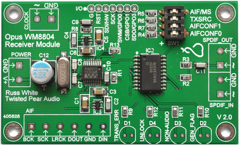
On the board above, the "I/O" port goes as follows: GSSSSSSSSS where G is gound and S is signal. In general, you need at least one ground wire for each signal wire, and need to arrange them in "GSGSGSGSGSG"-style on the cable.
Connector should look like this:
SSSSSSSSSSS
GGGGGGGGGGG
OR
GSGSGSGSGSGSG
Your's B3's ports look better, in
SSSSSSSSSSS
GGGGGGGGGGG
style, but i'm not 100% sure the second row of each port is connected to ground. Check it out, and if they are connected to ground, use flat ribbon cables, and stick every 2nd wire into GND pad.
See attatched.
The copper foil is soldered to "pad" on the pcb, near I2S connector, and then being sticked to I2S wires + wrapping around wires.
The issue looks this way:
On the board above, the "I/O" port goes as follows: GSSSSSSSSS where G is gound and S is signal. In general, you need at least one ground wire for each signal wire, and need to arrange them in "GSGSGSGSGSG"-style on the cable.
Connector should look like this:
SSSSSSSSSSS
GGGGGGGGGGG
OR
GSGSGSGSGSGSG
Your's B3's ports look better, in
SSSSSSSSSSS
GGGGGGGGGGG
style, but i'm not 100% sure the second row of each port is connected to ground. Check it out, and if they are connected to ground, use flat ribbon cables, and stick every 2nd wire into GND pad.
Attachments

Hey S3etup
Thanks for that, much clearer, picture paints a thousand pixels, probably more....
I am looking to use the u.fl connectors for the I2S to the BIII, thoughts on these? Will check the grounds as you advise, will see how I can fit the copper foil....
Thanks again,
Drew.
Thanks for that, much clearer, picture paints a thousand pixels, probably more....
I am looking to use the u.fl connectors for the I2S to the BIII, thoughts on these? Will check the grounds as you advise, will see how I can fit the copper foil....
Thanks again,
Drew.
I've gone SMA myself, as these are crimpable, and easily obtainable connectors.
I do the I2S wires as described above, but these I2S wires go to the DFF reclocker on DAC's board, which gets it's clock from SMA. It's the cheapest way i could think of for maintaining best I2S signal's shape jitterwise - after reclocker.
u.fl are fine as long as you don't need to reconnect them several times (i've heard they would break). They should be much better than ribbon cables.
I've gone SMA myself, as these are crimpable, and easily obtainable connectors.
I do the I2S wires as described above, but these I2S wires go to the DFF reclocker on DAC's board, which gets it's clock from SMA. It's the cheapest way i could think of for maintaining best I2S signal's shape jitterwise - after reclocker.
u.fl are fine as long as you don't need to reconnect them several times (i've heard they would break). They should be much better than ribbon cables.
no actually u.fl are much hardier than people think if you handle then correctly and besides if you are doing lots of disconnect cycles for initial testing perhaps just use the ribbon (hardwired with minimal solder at dac end) for that and then use u.fl after youve confirmed correct operation, you should be planning your layout thoroughly beforehand anyway. pretty easy to replace anyway, particularly here when you are only using 1 x ring and the center.
but yeah as long as you dont try to just disconnect them by just pulling them off they'll actually last quite well. definitely either buy the disconnection tool, or fashion your own
Examples...
Hi,
This is a very useful thread - thanks for the contributions - it's made great reading and I keep coming back to it to dip into the resources Marce posted.
Thanks !
I wonder if anyone would be willing to have a quick look at this and answer some very simple yes/no questions.
It is an example of what, to me, looks like routing that needs to be much improved. Is it very bad, bad, okay, or not-to-worry ? I know it's not great.
There are numerous kinks and vias and the terminating resistors, although smd, are at the receiving end.
The transmitter is Altera Cyclone III EP3C16. The datasheet says Iout for each pin is 40mA, which seems quite high to me, but basically it seems to be quite a low impedance output. Have I understood this correctly ? Does this mean the routing and termination are acceptable ?
http://www.altera.co.uk/literature/hb/cyc3/cyc3_ciii52001.pdf
Thanks for any comments. Much appreciated !
Hi,
This is a very useful thread - thanks for the contributions - it's made great reading and I keep coming back to it to dip into the resources Marce posted.
Thanks !
I wonder if anyone would be willing to have a quick look at this and answer some very simple yes/no questions.
It is an example of what, to me, looks like routing that needs to be much improved. Is it very bad, bad, okay, or not-to-worry ? I know it's not great.
There are numerous kinks and vias and the terminating resistors, although smd, are at the receiving end.
An externally hosted image should be here but it was not working when we last tested it.
The transmitter is Altera Cyclone III EP3C16. The datasheet says Iout for each pin is 40mA, which seems quite high to me, but basically it seems to be quite a low impedance output. Have I understood this correctly ? Does this mean the routing and termination are acceptable ?
http://www.altera.co.uk/literature/hb/cyc3/cyc3_ciii52001.pdf
Thanks for any comments. Much appreciated !
Last edited:

Without the schematic and knowing what the devices are I could not comment on the placement of the resistors, though series should always be at the transmitter end.
As to the routing; there is nothing basicly wrong with the signal routing, it looks like any standard digital board. What are your concerns with the signal routing?
What would be of concern to me and would require sorting is the copper pour (GND) between the signals, if you look closely you will notice that there are numerous slivers of copper pour that do not have stiching vias at least at each end, these for dipole structures on the board, not good for emc.
So to sumerise, the signal routing is standard for digital, it will not cause any problems whatsoever, the ground copper pour though does not have enough stiching vias (to one would hope a full contigous ground plane on an inner layer) and there are long slivers that have only a via at one end.
Thanks
Thanks for the reply.
My concerns are really because it is a high data rate, a 2-layer (probably cheap) PCB, the terminating resistors are quite large (100ohm), and there are numerous kinks and vias.
I saw the gnd pours and I hoped these would be beneficial but perhaps it'll need some work. I have a scope but only 12Mhz, so it might be tricky to improve it if it's a lemon.
I'll give it a go though.
Thanks again for the comments.
Its not going to have to high a data rate, so I would worry to much on that score. If the waves look OK (dont forget to take into account your scope probe loading) then I wouldn't worry.
Series resistors are there to match the signal to the layout topography, so there is realy no off the shelf value, it depend on the layout topography andf impedance, there are only two ways to determine the value:
Simulate the design using signal integrity tools and choose the best value, or try different values and see which gives the best measured result. Attached are some screen shots showing the actual difference different values of series resistors make, in this case 82R was chosen.
Vias and Kinks in traces will have no noticable effect on signal integrity at frequencies and rise time the DIYer is gonna be playing with, but with good layout you can minimise the number of layer changes a signal has between A & B.
My main concern would be a two layer board, these days ALL digital designs should be 4 layers min, with a full contigous ground plane. The main problem these days is signal rise time, which are forever getting faster and faster, and ultimetly it is the rise time of a signal (suignals) that determine whether a design is high speed.
Yes ground pour help if they are done correctly and are a must for two layer digital boards, but they need lots of stiching vias to be of any use.
Attachments


Thanks again Marce. I've ordered the DAC and I'm getting the seller to build and test it. I'll post more info when it arrives.
Racer - I see your resistors are near the DAC IC. Naughty Denon ? ;-)
Racer - I see your resistors are near the DAC IC. Naughty Denon ? ;-)
A few related links, I have lots more regarding SIV etc:
http://www.ti.com/lit/an/spraak6/spraak6.pdf
http://www.ultracad.com/mentor/mentor termination placement.pdf
http://www.the-signal-and-power-int...te_Source_Termination_Resistor_Location_2.pdf
http://www.ti.com/lit/an/scaa082/scaa082.pdf
Sites for more in depth Signal Integrity guidelines
beTheSignal.com
Signal Consulting, Inc. - Dr. Howard Johnson
Another usfull site:
Welcome to the Signal Integrity Prescription Monthly Column With Dr. Eric Bogatin
No problem, I layout PCBs every day of the week and have done for over 25 years now, and do a lot of high speed, SMPS and hi reliability PCB layouts. I have always got this info to hand, not only for use at work, but for a PCB forum where we get asked the same questions repeatably.
- Status
- Not open for further replies.
- Home
- Source & Line
- Digital Line Level
- I2S and digital signal path - in-line resistors?