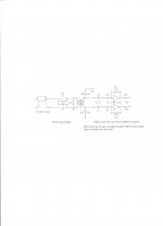
This buffered SPDIF input stage designed by Jocko Homo can avoid dropouts in my Buffalo III?
Rz 100R
R1 300R
Cz 4,7pF/5pF
Hex Inverter used Phillips 74HC04N instead of 74HCU04, operating voltage between +5V
Is there is a way to improve the schematic or needs other operating voltage, suggestions will welcome.
Rz 100R
R1 300R
Cz 4,7pF/5pF
Hex Inverter used Phillips 74HC04N instead of 74HCU04, operating voltage between +5V
Is there is a way to improve the schematic or needs other operating voltage, suggestions will welcome.
Attachments
Last edited:
Please help!
What about this circuit do you feel requires improvement, are you having some kind of trouble with it?
Perhaps you should try using the unbuffered 74HCU04. For this kind of analog applications the unbuffered version normally works better. Have you measured the output signals with an oscilloscope? Perhaps the buffered '04 generates additional transitions?
Does the circuit behind this require/tolerate a 0 to 5V signal?
Does the circuit behind this require/tolerate a 0 to 5V signal?
see i'm thinking there has to be something else going on here, i have no lock problems with my buff II, nor ackodac and I never have, yet you have had them consistently, to the point i wouldnt suggest for you to spend more money on the fifo just hoping to solve the problem when you do not really know what the problem is, only the result.
the jitter would have to be incredible to cause such a problem, i think you have some sort of electrical issue in your house that causes the unlock. does it not lock at all, or you have problems with it unlocking during use? dirty power spikes on the mains have been known to cause this sort of issue, as with ground loops.
the jitter would have to be incredible to cause such a problem, i think you have some sort of electrical issue in your house that causes the unlock. does it not lock at all, or you have problems with it unlocking during use? dirty power spikes on the mains have been known to cause this sort of issue, as with ground loops.
Perhaps you should try using the unbuffered 74HCU04. For this kind of analog applications the unbuffered version normally works better. Have you measured the output signals with an oscilloscope? Perhaps the buffered '04 generates additional transitions?
Does the circuit behind this require/tolerate a 0 to 5V signal?
First of all I don't be sure if I can use 74HC04N instead 74HCU04 for the attached schematic both voltage range 2V-6V
I don't know, the circuit behind is the Buffalo III.
If I'm not mistaken, Thorsten Loesch, for one, doesn't much care for this type of circuit at the S/PDIF input. I seem to recall him writing about how the output being coupled back to the input sends interference back up the S/PDIF line.
Have you tested the reciever for lock robustness with the logic inverters out of circuit?
Have you tested the reciever for lock robustness with the logic inverters out of circuit?
Last edited:
If k'm not mistaken, Thorsten Loesch doesn't much care for this type of circuit utilized at the S/PDIF input. I seem to recall him writing about how the fact that the output being coupled back to the input sends interference back up the S/PDIF line.
Have you tested it for lock robustness without the logic inverters in circuit?
Yes in BIII to setting the DPLL bandwith I used SW1 pins 5,6 & 7 ON position that's the highest setting this value will allow the DAC to get a lock to the incoming signal much easier, but at the same time it will allow more jitter to pass through but still have dropouts, tonight I will try default setting SW1 pins 5,6 & 7 OFF position, In ‘Default’ mode the DAC attempts to set the DPLL bandwidth automaticly. I will tell you how this setting goes.
@Ken
It does look more complicated than what is needed, but if it's what merlin el mango wants to try that's fine with me.
@ merlin el mango
The supply voltage for the buffered and un-buffered '04 may be the same, but that does not mean that their performance will be the same. The buffered version is not very good in this kind of circuit with an analog feedback. It could easily become unstable.
One thing that just struck me is that you might need to add a decoupling capacitor on the 5V supply, e.g. a 100nF ceramic capacitor with leads as short as possible. Such a capacitor is not shown on your schematic and it is not visible on the PCB either, but it could of course be hidden on the backside. If there is no decoupling capacitor you definitely need to add one. If there is no supply decoupling and you even use a buffered '04 there is a very high risk of instability, so perhaps you have got a signal on the output at several MHz?
If you need a TTL level input for the Buffalo I assume you actually only need one output.
@Ken
It does look more complicated than what is needed, but if it's what merlin el mango wants to try that's fine with me. Could you post other less complicated schematic to buffer the input S/PDIF or better to avoid jitter?
@ merlin el mango
The supply voltage for the buffered and un-buffered '04 may be the same, but that does not mean that their performance will be the same. The buffered version is not very good in this kind of circuit with an analog feedback. It could easily become unstable. OK I understand, but the question is: I need to buffer the S/PDIF or I ned to reduce the jitter, I mind that I need to reduce jitter, if so wich schematic can I to implement?
One thing that just struck me is that you might need to add a decoupling capacitor on the 5V supply, e.g. a 100nF ceramic capacitor with leads as short as possible. Such a capacitor is not shown on your schematic and it is not visible on the PCB either, but it could of course be hidden on the backside. If there is no decoupling capacitor you definitely need to add one. If there is no supply decoupling and you even use a buffered '04 there is a very high risk of instability, so perhaps you have got a signal on the output at several MHz? OK I solder 100nF directly at the Vcc & Gnd of 74HC04N
If you need a TTL level input for the Buffalo I assume you actually only need one output. Yes I need only one output
Answer in red.
Thanks for help.
A way to modify it could be as follows:
Short circuit R2.
Change R3 to 300ohm (I assume here that the impedances are optimized for use with this transformer).
Take the output from R9.
You can of course also remove C1, R4, R6 and R8 if you like, but it is not absolutely necessary, at least for a quick test.
See also: S/PDIF Digital to Analogue Converter
If the Buffalo III expects a 3V logic level perhaps you should also try to reduce the supply voltage from 5V to 3V or 3.3V
The proposed modification also has the advantage that you get twice as much signal available. This may in fact reduce the jitter to some degree. But the circuit will not really reduce the jitter. The best you can hope for is that the circuit will not add too much jitter. If you want to reduce the jitter you will need a receiver with a PLL or something similar, e.g. a Wolfson SPDIF receiver, but then it is of course a much more complicated design.
This buffered SPDIF input stage designed by Jocko Homo can avoid dropouts in my Buffalo III?
Rz 100R
R1 300R
Cz 4,7pF/5pF
Hex Inverter used Phillips 74HC04N instead of 74HCU04, operating voltage between +5V
Is there is a way to improve the schematic or needs other operating voltage, suggestions will welcome.
Hello
The output signal is inverted or not with this stage ?
Serge
This circuit has been proposed by Jocko Homo for the CS8412 / ..14 receiver chips, which have schmitt trigger inputs. Those schmitt trigger inputs can send back garbage, and the chip "liked" to be driven differentially.
Maybe you should check first what the ESS chip really likes to see at the input, and if there is a +RX and -RX pin for diff input. It could well be better to use a fast (video) opamp instead of the inverter.
Maybe you should check first what the ESS chip really likes to see at the input, and if there is a +RX and -RX pin for diff input. It could well be better to use a fast (video) opamp instead of the inverter.
This circuit has been proposed by Jocko Homo for the CS8412 / ..14 receiver chips, which have schmitt trigger inputs. Those schmitt trigger inputs can send back garbage, and the chip "liked" to be driven differentially.
Maybe you should check first what the ESS chip really likes to see at the input, and if there is a +RX and -RX pin for diff input. It could well be better to use a fast (video) opamp instead of the inverter.
Yes you have reason, I'm going in other direction: jitter reduction because I have TP S/PDIF-4 Input board for BIII & still I have dropouts

- Status
- This old topic is closed. If you want to reopen this topic, contact a moderator using the "Report Post" button.
- Home
- Source & Line
- Digital Line Level
- buffer SPDIF input stage for ESS9018