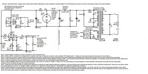
I decided to replace the analogue output stage of my AN DAC after a fault had developed. I could have repaired it but I've always considered the ECC88 SRPP as being a poor man's amplifier, and my junk box contained two excellent Sowter 8423 1:2 interstage transformers. I spoke to Sowter and was assured that these were fully symmetrical and would work equally well stepped down as long as 1ry and 2ry load impedances were properly balanced for optimum square wave response.
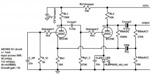
Seeking an overall gain of 30+ with low output impedance after step down, I needed common, low cost, high mu triodes with low rp to drive these, and targeted EF184 and EF80. I bought four NOS Siemens EF80, four NOS Mullard EF184 and later, six NOS Mullard EF80.
I originally designed the circuit triode wired to accept both valve types although the load line was better matched for the EF80s and any rogue EF184s were liable to run a little hot with the chosen bias voltage. There were sonic differences between valve types and I favoured the EF80. There were also sonic differences between makes of EF80 and, after seeing nothing to account for this on my home brew valve tester, I felt that there must be some shortcoming in the circuit causing this.
I knew that Pentode operation is more immune to the effects of input transients if driving capacitative loads (Valve Operating Conditions, Wireless Engineer, Vol. XXVIII, July 1951, No. 334) and has lower distortion at low output levels. Since pentode mode rp is high, a transformer primary load resistor was required in addition to the usual secondary load resistor to provide balanced transformer loading with optimum square wave amplification (where valves are triode
wired, this primary load resistor is traditionally omitted since low triode rp is effectively in parallel with the primary, albeit through the power supply).
Pentode operation sounded much cleaner. Capacitors were added as precautionary measures to prevent any high frequency parasitic oscillations and this appeared to minimise sonic differences between Siemens and Mullard EF80.
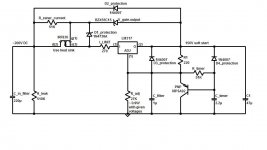
I wanted some voltage regulation in the power supply since the EF80s were fixed bias at around 1.62V using Avago HLMP6000. The output voltage of the junk box 154V-0-154V Sowter 0211 mains transformer I'd had specially made for a different project was a little too low for a valve rectifier with guaranteed striking of VR150 regulators so I opted for semiconductor diodes. Junk box Sowter CB25 chokes provided the necessary smoothing with minimum voltage drop. The RC filter following the VR150 is designed for cross over at f-3dB of ~100Hz.
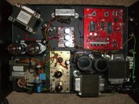
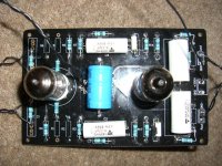
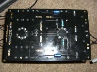
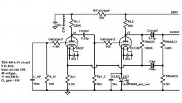
I've attached a photo, the circuit diagram and LED VI curve for my junk box AD1865 DAC amp which, in my opinion, is sonically far superior to the SRPP.
I've been using this for well over a year now and the only downside I can see is the expense of it.
I recently renovated a pair of QUAD II power amps, a QUAD 22 control unit and QUAD FM tuner with multiplex decoder, replacing all resistors and capacitors (and realigning the tuner + MPX). This gave me the opportunity to compare my EF80 DAC amp back to back with the 2 x ECC83 feedback preamp in the QUAD 22. With volumes carefully matched, I preferred my EF80 amp 70% of the time during blind testing with my son in control of the switch over, but I was impressed how remarkably similar they sounded. My son couldn't tell the difference. Both used the AD1865 DAC with 56R load resistor as source and there was some minor earth loop hum present.
Inspired by the fact that, in all probability, they must both be close to being right because of their very different design yet sonic similarity, I thought I should re-design the QUAD 22 preamp making it more suited to modern line output standards. If sonically similar, it would offer a very cheap alternative to my EF80 amp. My next post will provide details of my progress.
Seeking an overall gain of 30+ with low output impedance after step down, I needed common, low cost, high mu triodes with low rp to drive these, and targeted EF184 and EF80. I bought four NOS Siemens EF80, four NOS Mullard EF184 and later, six NOS Mullard EF80.
I originally designed the circuit triode wired to accept both valve types although the load line was better matched for the EF80s and any rogue EF184s were liable to run a little hot with the chosen bias voltage. There were sonic differences between valve types and I favoured the EF80. There were also sonic differences between makes of EF80 and, after seeing nothing to account for this on my home brew valve tester, I felt that there must be some shortcoming in the circuit causing this.
I knew that Pentode operation is more immune to the effects of input transients if driving capacitative loads (Valve Operating Conditions, Wireless Engineer, Vol. XXVIII, July 1951, No. 334) and has lower distortion at low output levels. Since pentode mode rp is high, a transformer primary load resistor was required in addition to the usual secondary load resistor to provide balanced transformer loading with optimum square wave amplification (where valves are triode
wired, this primary load resistor is traditionally omitted since low triode rp is effectively in parallel with the primary, albeit through the power supply).
Pentode operation sounded much cleaner. Capacitors were added as precautionary measures to prevent any high frequency parasitic oscillations and this appeared to minimise sonic differences between Siemens and Mullard EF80.
I wanted some voltage regulation in the power supply since the EF80s were fixed bias at around 1.62V using Avago HLMP6000. The output voltage of the junk box 154V-0-154V Sowter 0211 mains transformer I'd had specially made for a different project was a little too low for a valve rectifier with guaranteed striking of VR150 regulators so I opted for semiconductor diodes. Junk box Sowter CB25 chokes provided the necessary smoothing with minimum voltage drop. The RC filter following the VR150 is designed for cross over at f-3dB of ~100Hz.
I've attached a photo, the circuit diagram and LED VI curve for my junk box AD1865 DAC amp which, in my opinion, is sonically far superior to the SRPP.
I've been using this for well over a year now and the only downside I can see is the expense of it.
I recently renovated a pair of QUAD II power amps, a QUAD 22 control unit and QUAD FM tuner with multiplex decoder, replacing all resistors and capacitors (and realigning the tuner + MPX). This gave me the opportunity to compare my EF80 DAC amp back to back with the 2 x ECC83 feedback preamp in the QUAD 22. With volumes carefully matched, I preferred my EF80 amp 70% of the time during blind testing with my son in control of the switch over, but I was impressed how remarkably similar they sounded. My son couldn't tell the difference. Both used the AD1865 DAC with 56R load resistor as source and there was some minor earth loop hum present.
Inspired by the fact that, in all probability, they must both be close to being right because of their very different design yet sonic similarity, I thought I should re-design the QUAD 22 preamp making it more suited to modern line output standards. If sonically similar, it would offer a very cheap alternative to my EF80 amp. My next post will provide details of my progress.
Attachments
Using an I/V resistor greater than 56 ohms would make it possible to consider a number of excellent sounding lower mu triodes. I find that the AD1865 sounds very clean with a passive resistor I/V as high as 330ohms. I settled on 191 ohms in my own AD1865 based diy DAC.
Last edited:
Hi Ken,
I remember reading that some prefer the sound when IV resistor is high but this doesn't seem logical unless the power supply can't deliver a whopping 1mA of current – or maybe it's some limitation of the high mu valve amps they tried. It's something I wanted to experiment with but it's a bit late just now. I've already designed and built a prototype of the feedback DAC amp with a gain of ~33 to match the gain of the EF80 DAC amp so they'll be compared using 56R IV. I've got it working and briefly auditioned it, but it's not ready yet. I need to break the ground tracks on the PCB I bought and properly star ground it, and then provide independent power supplies so I can switch between to two for comparison.
I'll try to document the design tomorrow. I want to demonstrate the development stages using LTSPICE but I'm aware that most people don't use it. Fairly new to it myself. Does anyone know how to capture the black screen plots for upload rather than the .asc file?
Did you document your DAC design, Ken?
Regards,
Bob
Hi, Valveuser,
The choice to use an larger rather than smaller value I/V resistor is one not so much based on the feeling that a larger value sounds better, but that it affords one the option to use a lower gain lower feedback output amplifier, or even no output amplifer at all. The important thing regarding I/V resistor value and the AD1865, as well as PCM56 and TDA1543, is that they are current output DACs having sufficient output voltage compliance to enable the choice of a relatively large value resistor without incurring perceptable distortion or other degradation. The AD1865's 1mA peak ouput current is not germaine is this case.
No, I haven't published my DIY DAC design becuase it is mostly a platform for my experimentation. With it, I've been able to evaluate OS, NOS, and apodized OS via a programmable digital filter, and op-amp I/V versus passive resistor I/V as well. As far as I/V is concerned, I found passive resistor direct output (no output amp, direct to a line preamp) to sound best.
Last edited:
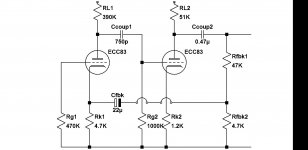
[FONT=Times New Roman, serif]Stripped to its bare essentials, the building block of the QUAD 22 preamp would look like the first attachment, except that I've thrown in different (not optimised) component values solely for the purpose of discussion.[/FONT]
[FONT=Times New Roman, serif]Since it's an old and classic QUAD design, I thought it appropriate to give credits to other original pioneers where possible. [/FONT]
[FONT=Times New Roman, serif]The circuit is a form of Duerdoth's multiple feedback involving both current and voltage feedback which must be added together to determine overall performance. E. Watkinson derived equations which partially describe the modified circuit (Radiotron Designer's Handbook, F. Langford-Smith, 4th Edition, Chapter 7.2 vi). [/FONT]
[FONT=Times New Roman, serif]In the first instance, note that all capacitors are included in the feedback loop, minimising their sonic colouration. [/FONT]
[FONT=Times New Roman, serif]According to J.E. Flood, Wireless Engineer, July 1950, pp 201-209, the Critical Damping condition is met for two f-3dB cut-off frequencies without a compensated feedback path when; [/FONT]
[FONT=Times New Roman, serif](1 - ßA) = (f-3dB_1 + f-3dB_2)² / (4 x f-3dB_1 x f-3dB_2)[/FONT]
[FONT=Times New Roman, serif]or, given (1-ßA), the ratio[/FONT]
[FONT=Times New Roman, serif](f-3dB_2 / f-3dB_1) = (2 x (1 - ßA)) - 1 + (sqrt(((4 x (1 - ßA)2) - (4 x (1 - ßA))))[/FONT]
[FONT=Times New Roman, serif]He also describes conditions to avoid valve overloading, Wireless Engineer, August 1952, pp 203-212.[/FONT]
[FONT=Times New Roman, serif]For HF, (f-3dB_2) ≥ (f-3dB_1)(1 - ßA) and for LF, (f-3dB_1) ≥ (f-3dB_2)(1 - ßA) to avoid 2nd stage valve overloading.[/FONT]
[FONT=Times New Roman, serif]I created a spreadsheet but don't want to get involved in the mathematics here since the number crunching can be done using SPICE. Instead, I hope a brief description will suffice. [/FONT]
[FONT=Times New Roman, serif]In the HF design, f-3dB_1 is lowered by using un-bypassed Rk1 which provides local current feedback and consequently high rp1', in addition to high RL1, high Rg2 and high V2 Miller capacitance. As a result of this, it's an unfortunate compromise that V1 operates near starvation conditions. A pentode would be a better solution but adds an extra valve. Staggering is relative to f-3dB_2, i.e. rp2', RL2, Rvol, and series Rfbk1 + Rfbk2, and the output capacitance. Given that interconnect and power amp input capacitances are more or less fixed, rp2' and RL2 should ideally be low, placing less demand on the requirement to lower f-3dB_1 for a given stagger ratio, as well as lowering output impedance. Therefore, the use of an LED for fixed bias of V2 instead of Rk2 is the basis of the first modification. [/FONT]
[FONT=Times New Roman, serif]Since V1 operates with low current and V2 with high, their ground currents should be kept separate on a PCB. [/FONT]
[FONT=Times New Roman, serif]The LF design is complicated a little with an extra time constant which, for all practical purposes, can be ignored if Cfbk is made sufficiently large - there is limited freedom to alter Rk1 and Rfbk2. For a given feedback factor, Rfbk1 also now becomes fixed and the necessary staggering can only be realistically achieved by making Ccoup1 small relative to Ccoup2 given that Rg2, rp1' and RL1 have already been set to satisfy HF staggering. Ccoup2 must be kept reasonably small to avoid switch-on and switch-off voltage surges at the output, and 0.47u would be a sensible maximum. Ccoup1 is therefore abnormally small, a frustrating compromise which invites stray capacitance effects and limits the closed loop LF f-3dB. [/FONT]
[FONT=Times New Roman, serif]It's these compromises in the LF design which prompted the second modification, that of subsidiary DC feedback. This then demands a regulated power supply but allows the use of a normal capacitance value for Ccoup1 and improves LF f-3dB considerably. [/FONT]
[FONT=Times New Roman, serif]Since rp1' = rp + (Rk1 x [FONT=Times New Roman, serif]μ[/FONT]1), V1 doesn't need to have the high rp of ECC83 provided [FONT=Times New Roman, serif]μ1[/FONT] and Rk1 are sufficiently high. The main requirement is that the VI characteristics don't show significant curvature near cut off even though current feedback will straighten and flatten the curves out to a considerable extent. Most triodes don't meet this requirement but ECC83, 6SL7 and ECC88 and their variants generally do above ~250uA. 6N2P is cheap with a useful 6V3 heater voltage. [/FONT]
[FONT=Times New Roman, serif]I curve traced about a dozen NOS ECC88s and they were consistently good candidates for V1. Since the low rp requirement for V2 is also met, ECC88 was selected for the prototype design. [/FONT]
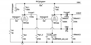
[FONT=Times New Roman, serif]Next attachment shows circuit diagram with 2nd stage fixed bias. Anode stoppers weren't used since the PCB didn't support this and they are only needed where RL is remote from anode, or anode is connected to low impedance, e.g. in cathode follower. [/FONT]
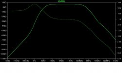
[FONT=Times New Roman, serif]Next is amplitude frequency response with 2nd stage fixed bias.[/FONT]
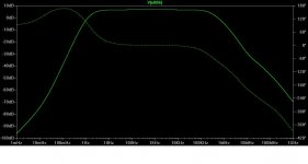
[FONT=Times New Roman, serif]Next is circuit diagram with additional DC feedback. Note conventionally sized coupling capacitors. [/FONT]
[FONT=Times New Roman, serif]Next is amplitude phase with additional DC feedback. Note improved low frequency response.[/FONT]
[FONT=Times New Roman, serif]Last attachments show prototype on PCB which required several alterations. Ground tracks need breaking and star grounding. [/FONT]
[FONT=Times New Roman, serif]Link to PCB used [/FONT]
[FONT=Times New Roman, serif]http://www.diyaudio.com/forums/tubes-valves/197400-12ax7-12au7-preamp.html[/FONT]
[FONT=Times New Roman, serif]Since it's an old and classic QUAD design, I thought it appropriate to give credits to other original pioneers where possible. [/FONT]
[FONT=Times New Roman, serif]The circuit is a form of Duerdoth's multiple feedback involving both current and voltage feedback which must be added together to determine overall performance. E. Watkinson derived equations which partially describe the modified circuit (Radiotron Designer's Handbook, F. Langford-Smith, 4th Edition, Chapter 7.2 vi). [/FONT]
[FONT=Times New Roman, serif]In the first instance, note that all capacitors are included in the feedback loop, minimising their sonic colouration. [/FONT]
[FONT=Times New Roman, serif]According to J.E. Flood, Wireless Engineer, July 1950, pp 201-209, the Critical Damping condition is met for two f-3dB cut-off frequencies without a compensated feedback path when; [/FONT]
[FONT=Times New Roman, serif](1 - ßA) = (f-3dB_1 + f-3dB_2)² / (4 x f-3dB_1 x f-3dB_2)[/FONT]
[FONT=Times New Roman, serif]or, given (1-ßA), the ratio[/FONT]
[FONT=Times New Roman, serif](f-3dB_2 / f-3dB_1) = (2 x (1 - ßA)) - 1 + (sqrt(((4 x (1 - ßA)2) - (4 x (1 - ßA))))[/FONT]
[FONT=Times New Roman, serif]He also describes conditions to avoid valve overloading, Wireless Engineer, August 1952, pp 203-212.[/FONT]
[FONT=Times New Roman, serif]For HF, (f-3dB_2) ≥ (f-3dB_1)(1 - ßA) and for LF, (f-3dB_1) ≥ (f-3dB_2)(1 - ßA) to avoid 2nd stage valve overloading.[/FONT]
[FONT=Times New Roman, serif]I created a spreadsheet but don't want to get involved in the mathematics here since the number crunching can be done using SPICE. Instead, I hope a brief description will suffice. [/FONT]
[FONT=Times New Roman, serif]In the HF design, f-3dB_1 is lowered by using un-bypassed Rk1 which provides local current feedback and consequently high rp1', in addition to high RL1, high Rg2 and high V2 Miller capacitance. As a result of this, it's an unfortunate compromise that V1 operates near starvation conditions. A pentode would be a better solution but adds an extra valve. Staggering is relative to f-3dB_2, i.e. rp2', RL2, Rvol, and series Rfbk1 + Rfbk2, and the output capacitance. Given that interconnect and power amp input capacitances are more or less fixed, rp2' and RL2 should ideally be low, placing less demand on the requirement to lower f-3dB_1 for a given stagger ratio, as well as lowering output impedance. Therefore, the use of an LED for fixed bias of V2 instead of Rk2 is the basis of the first modification. [/FONT]
[FONT=Times New Roman, serif]Since V1 operates with low current and V2 with high, their ground currents should be kept separate on a PCB. [/FONT]
[FONT=Times New Roman, serif]The LF design is complicated a little with an extra time constant which, for all practical purposes, can be ignored if Cfbk is made sufficiently large - there is limited freedom to alter Rk1 and Rfbk2. For a given feedback factor, Rfbk1 also now becomes fixed and the necessary staggering can only be realistically achieved by making Ccoup1 small relative to Ccoup2 given that Rg2, rp1' and RL1 have already been set to satisfy HF staggering. Ccoup2 must be kept reasonably small to avoid switch-on and switch-off voltage surges at the output, and 0.47u would be a sensible maximum. Ccoup1 is therefore abnormally small, a frustrating compromise which invites stray capacitance effects and limits the closed loop LF f-3dB. [/FONT]
[FONT=Times New Roman, serif]It's these compromises in the LF design which prompted the second modification, that of subsidiary DC feedback. This then demands a regulated power supply but allows the use of a normal capacitance value for Ccoup1 and improves LF f-3dB considerably. [/FONT]
[FONT=Times New Roman, serif]Since rp1' = rp + (Rk1 x [FONT=Times New Roman, serif]μ[/FONT]1), V1 doesn't need to have the high rp of ECC83 provided [FONT=Times New Roman, serif]μ1[/FONT] and Rk1 are sufficiently high. The main requirement is that the VI characteristics don't show significant curvature near cut off even though current feedback will straighten and flatten the curves out to a considerable extent. Most triodes don't meet this requirement but ECC83, 6SL7 and ECC88 and their variants generally do above ~250uA. 6N2P is cheap with a useful 6V3 heater voltage. [/FONT]
[FONT=Times New Roman, serif]I curve traced about a dozen NOS ECC88s and they were consistently good candidates for V1. Since the low rp requirement for V2 is also met, ECC88 was selected for the prototype design. [/FONT]
[FONT=Times New Roman, serif]Next attachment shows circuit diagram with 2nd stage fixed bias. Anode stoppers weren't used since the PCB didn't support this and they are only needed where RL is remote from anode, or anode is connected to low impedance, e.g. in cathode follower. [/FONT]
[FONT=Times New Roman, serif]Next is amplitude frequency response with 2nd stage fixed bias.[/FONT]
[FONT=Times New Roman, serif]Next is circuit diagram with additional DC feedback. Note conventionally sized coupling capacitors. [/FONT]
[FONT=Times New Roman, serif]Next is amplitude phase with additional DC feedback. Note improved low frequency response.[/FONT]
[FONT=Times New Roman, serif]Last attachments show prototype on PCB which required several alterations. Ground tracks need breaking and star grounding. [/FONT]
[FONT=Times New Roman, serif]Link to PCB used [/FONT]
[FONT=Times New Roman, serif]http://www.diyaudio.com/forums/tubes-valves/197400-12ax7-12au7-preamp.html[/FONT]
Attachments
-
 QUAD type schematic.JPG95 KB · Views: 1,253
 -
 ECC88 critical damping schematic.JPG53.6 KB · Views: 1,235
 -
 ECC88 critical damping amplitude phase.JPG38.6 KB · Views: 372
 -
 ECC88 critical damping subsidiary DC fbk schematic.JPG135 KB · Views: 456
 -
 ECC88 critical damping subsidiary DC fbk amplitude phase.JPG39.9 KB · Views: 373
 -
 PCB top.jpg146.4 KB · Views: 268
 -
 PCB bottom.jpg72.8 KB · Views: 288
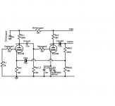
The ECC88s needed 1K5 grid stopper resistors fitted right at the valve bases (ECC88 SRPP owners please note). The first attachment shows the circuit diagram.
The second attachment shows the 157V soft start LM317 regulated power supply shared by both channels.
For convenience, a regulated DC heater supply was used with -ve tied to star ground.
MKP capacitors were used for coupling and LED HF bypass and, where available, long life electrolytic capacitors were used elsewhere - all certified free from fairy dust. Feedback virtually eliminates sonic colourations from capacitors and valves (NOS Tesla ECC88 used here).
With an output load of 50K and ~100pF interconnect + oscilloscope lead capacitance, 1KHz square wave response was as perfect as my hand held oscilloscope could resolve with no overshoot, ringing or sluggish rise time.
Output hum level was under ~0.3mV without special precautions (after 1K5 grid stoppers were fitted) but the preamp would benefit from RF screening inside a metal enclosure due to the high first stage impedances.
Bandwidth was very broad, measured at 1Hz to 120KHz (oscilloscope HF roll off was significant).
The next attachment is the .asc file. I've included ECC88 and Avago HLMP6000_std_red LED models as SPICE directives on the schematic, but you'll need to copy triode.asy (zip attached) into lib\sym\misc – see;
LTSpice and vacuum tube models
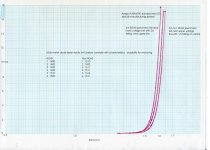
The ECC88 model was tweaked from N. Koren's data and you may wish to re-insert his parameters. From my own curve tracing experiences, Norman's choice of a lower μ of 28 is probably more realistic for ECC88. The Avago HLMP6000_std_red LED model is my own creation (I had to write a quick and dirty programme to determine IS and N parameters resulting in best fit with the VI curve I traced).
So, how did it compare to my EF80 DAC amp, played through QUAD 2 power amps and PMC FB1 speakers?
I made arrangements for switching between the two, both using the same digital source into 56R. I played a 1KHz sine wave MP3 file through the DAC, and matched RH channel volumes using an oscilloscope. As anticipated, LH channel level was the same for the feedback amp but a little out (~6% lower) for the EF80 amp due to minor gain differences.
In order to switch from my normal listening position, I had to use long interconnects with a total capacitance of ~350pF but this wouldn't be audible because output impedances of the ECC88 feedback, and EF80 DAC amps are estimated at ~0.5K and 2K5 respectively.
Switching appeared almost seamless and it was felt that such small differences may have gone unnoticed if there had been delays in between comparative listening tests. It took some time to note that the EF80 amp was a little lean in the lower middles, and it was speculated that this may be a result of the Mullard EF80's very slight sonic colouration in the non feedback circuit designed to minimise this, as previously discussed.
The Mullard EF80s were replaced with Siemens EF80s and the test procedure repeated. The channel balance difference was ~5% with the Siemens, again LH down. I couldn't distinguish between the EF80 and the ECC88 feedback DAC amps this time.
I concluded that the Siemens EF80 valves are more accurate than the Mullards in this circuit. If I remember correctly, they had very different sonic colourations before I changed to pentode operation and added G2 stoppers, local G2 capacitors and LED bypass capacitors, and I suspect that parasitic oscillations cause this colouration. It might be worth adding anode stopper resistors to see if the Mullards can be fully tamed but I'm more interested in fitting the ECC88 feedback amp in the same enclosure with switching options.
To summarise, I've achieved my goal to design a much cheaper AD1865 DAC amp and it's very satisfying that the two completely different designs sound essentially identical.
Bob
The second attachment shows the 157V soft start LM317 regulated power supply shared by both channels.
For convenience, a regulated DC heater supply was used with -ve tied to star ground.
MKP capacitors were used for coupling and LED HF bypass and, where available, long life electrolytic capacitors were used elsewhere - all certified free from fairy dust. Feedback virtually eliminates sonic colourations from capacitors and valves (NOS Tesla ECC88 used here).
With an output load of 50K and ~100pF interconnect + oscilloscope lead capacitance, 1KHz square wave response was as perfect as my hand held oscilloscope could resolve with no overshoot, ringing or sluggish rise time.
Output hum level was under ~0.3mV without special precautions (after 1K5 grid stoppers were fitted) but the preamp would benefit from RF screening inside a metal enclosure due to the high first stage impedances.
Bandwidth was very broad, measured at 1Hz to 120KHz (oscilloscope HF roll off was significant).
The next attachment is the .asc file. I've included ECC88 and Avago HLMP6000_std_red LED models as SPICE directives on the schematic, but you'll need to copy triode.asy (zip attached) into lib\sym\misc – see;
LTSpice and vacuum tube models
The ECC88 model was tweaked from N. Koren's data and you may wish to re-insert his parameters. From my own curve tracing experiences, Norman's choice of a lower μ of 28 is probably more realistic for ECC88. The Avago HLMP6000_std_red LED model is my own creation (I had to write a quick and dirty programme to determine IS and N parameters resulting in best fit with the VI curve I traced).
So, how did it compare to my EF80 DAC amp, played through QUAD 2 power amps and PMC FB1 speakers?
I made arrangements for switching between the two, both using the same digital source into 56R. I played a 1KHz sine wave MP3 file through the DAC, and matched RH channel volumes using an oscilloscope. As anticipated, LH channel level was the same for the feedback amp but a little out (~6% lower) for the EF80 amp due to minor gain differences.
In order to switch from my normal listening position, I had to use long interconnects with a total capacitance of ~350pF but this wouldn't be audible because output impedances of the ECC88 feedback, and EF80 DAC amps are estimated at ~0.5K and 2K5 respectively.
Switching appeared almost seamless and it was felt that such small differences may have gone unnoticed if there had been delays in between comparative listening tests. It took some time to note that the EF80 amp was a little lean in the lower middles, and it was speculated that this may be a result of the Mullard EF80's very slight sonic colouration in the non feedback circuit designed to minimise this, as previously discussed.
The Mullard EF80s were replaced with Siemens EF80s and the test procedure repeated. The channel balance difference was ~5% with the Siemens, again LH down. I couldn't distinguish between the EF80 and the ECC88 feedback DAC amps this time.
I concluded that the Siemens EF80 valves are more accurate than the Mullards in this circuit. If I remember correctly, they had very different sonic colourations before I changed to pentode operation and added G2 stoppers, local G2 capacitors and LED bypass capacitors, and I suspect that parasitic oscillations cause this colouration. It might be worth adding anode stopper resistors to see if the Mullards can be fully tamed but I'm more interested in fitting the ECC88 feedback amp in the same enclosure with switching options.
To summarise, I've achieved my goal to design a much cheaper AD1865 DAC amp and it's very satisfying that the two completely different designs sound essentially identical.
Bob
Attachments
Bob, I like the concept of two tube gain stages with fb for an analog DAC stage. With quiet tubes one could adapt it to possible the more troublesome DAC that need a lower IV resistor.
Now my issue with a tube analog out from a DAC has always been too much
2H for use with a following tube amp, things tend to get too soft. For me they work well with a SS main amp , probably because tubes done right generally handle the rf that poors out of DAC's well. As far as the channel mismatch that can be inevitable with tube, a decent work around is adjusting the I/V resistor.
So using feedback like you are doing I'm thinking the thd should be significantly better than my experiments, have you taken measurements?
Last edited:
Hi, Regal.
I prefer the ECC88 feedback design to the expensive EF80 transformer output design. Precise channel matching, lower sonic colourations and output impedance etc. Theoretically, it's a much better amp. Harmonic measurements would be interesting but, unfortunately, I don't have the equipment to measure them and, personally, I'd expect them to be inaudible here. I'd be inclined to describe the sound of this feedback design through a valve amp as accurate, rather than a soft, probably because of its wide bandwidth.
One of the reasons I chose the ECC88 input stage was to cut down on the overall gain such that a reasonable feedback factor could be used. I can very quickly re-design it for use with other input and output valves with different gains or feedback factors, etc. For example, it's a very simple matter to design a 6N2P input, ECC88 output variant with a CL gain of around 100. Just specify the CL gain requirements for your “troublesome” DAC and I'll see what I can come up with. The high stability margin of the design can also accommodate very large feedback factors with CL gain around 5 or possibly lower, and there's also a very considerable amount of headroom in the stages.
I bought two PCBs and it would be interesting to try a second one with a different digital section, but I'm not familiar with the spectrum of good quality DACs available and their output currents/voltages.
Regards,
Bob
The Audial website blog sums up the chips you should consider better than I can:
And classic multibit D/A chips story mostly stopped in 90s. Philips in fact stopped in 80s with TDA1541A, ADI stopped with AD1862, and the only remaining multibit representatives are Texas Instruments (Burr-Brown) PCM1702/1704, which were also designed back in 90s. Each of these chips should be considered not one simple point in DAC history, but the end and crown of its own era.
Thanks for the summary, Regal. I've looked at the data sheets and attached a schematic for a possible (untested) design, but first a progress update of the 2 x ECC88 design.
I managed to squeeze it into the same enclosure as the EF80 amp, positioning it above the cold part of the AD1865 PCB with an earthed copper screen in between them. Star earthing of both the ECC88 and the EF80 amps proved problematic with hum pick up so PCB earth connections were returned to original design and alternative arrangements were made. There's still a temporary but annoying 100Hz hum predominantly on one channel which only occurs with a cold start. I guess it's a layout issue and it falls below ~0.3mV after a minute or so.
I fitted 3n3 polypropylene capacitors between pins 4 and 5 of each valve to prevent any high frequency feedback through the heaters. This isn't shown on the previous schematics but is considered essential and is commonly seen in good quality FM tuner schematics. Where heaters have CT tied to (preferably above) ground, two series connected capacitors should be used for each valve as voltage dividers to CT, and they should be connected as close as possible to the valve base pins.
Alternative high gain design for difficult DACs.
The TDA1541A data sheet is unique in that it specifies output voltage compliance (+/- 25mV) as well as output current (0 to 4mA, presumably with digital silence at +2mA) so, if I have this right, 12R5 is the maximum I/V resistor value and, using this value, a gain of 113 is needed for 2VRMS output. There's also a +25mV DC offset at the input although this is essentially insignificant in this design with regard to first stage biasing.
I've chosen 100n RF filter capacitor (C_HF) which, in parallel with 12R I/V resistor, gives f-3dB of 133K but I suspect this isn't desirable as seen from TDA1541A's perspective. Gstopper1 combined with V1's Miller input capacitance also provides RF filtering with minimal effect on TDA 1541A. Some experimentation will be required and a Gstopper1 value up to 10K might prove to be the best RF filter without the need for C_HF.
A 200V HT supply sets 6N2P bias ~ -1.4V, well clear of +ve Ig1 and Ia cut-off. The amp has CL gain ~100, feedback factor (current as well as voltage) of ~11 with output impedance ~0.7K. Although designed for TDA1541A, it should be suitable for all of the aforementioned DACs using an appropriate I/V resistor value. Note that these amps are non inverting and, with such high gain, I'd expect layout and screening to be fairly critical.
Attachments
It turns out the TDA1541A data sheet confuses with regard to sign convention / offset currents / voltages and its -15V supply is a clue which I missed. Read -25mV offset instead of +25mV posted earlier. It's still insignificant here though.
It's quiet and I'm going to wrap it up now. I'm tempted to try proper 44.1KHz notch filters in front of the preamp using old FM MPX passive techniques with typically >40dB suppression but I need to acquire components. I also wanted to design a really good pentode input stage for the preamp without the triode's compromises but, alas, Springtime beckons and technology moves on.
Best wishes to all.
Bob
Before I leave this, I thought I'd make corrections and add a little on reconstruction filters.
AD1865 expects an inverting stage at Iout for correct phase (see data sheet) but the EF80 preamp schematic shows both the EF80 and the transformers (lead wire colour code) inverting - the green and violet wires need to be reversed.
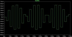
Here's a brief overview showing issues with NOS DACs;
http://myweb.tiscali.co.uk/g8hqp/audio/CDsample.html
I'm uncomfortable with the effects of these (inaudible) high frequency images on following equipment so I thought I'd simulate the DAC digital output signal using LTSPICE to assess different reconstruction filters in both the time and the frequency domains. I've attached the .asc file (44.1KHz sample & hold circuit followed by a voltage dependent current source into I/V resistor) but I've not included any candidate filters since this is a huge topic. I'm not sure if the modelling is strictly correct, but comparing FFT traces (with filter versus without filter), it appears that low order LCR low pass filters can remove the bulk of these images without the theoretical need for brick wall low pass filters which have characteristically high phase shifts inside the audio pass band compromising sound quality.
I'm not trying to advocate that this is the best solution. It's a compromise which has to be balanced against the brick wall filter requirement for 44.1KHz sampling frequency which compromised the NOS format's performance at design conception. I'm just investigating the minimum compromise necessary for the equipment I have.
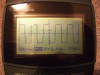
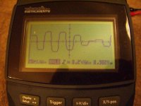
Fortunately, it turns out that my original EF80 preamp design is acceptable without additional low pass filtering because of its output transformers. I've now removed the ECC88 feedback preamp from the enclosure since there wasn't room for the filters that it required. I thought 20KHz scope traces might be of interest here.
With brick wall filter, time domain outputs should look like a normal 20KHz sine wave. Using low order filters, there will inevitably be a superimposed 44.1 – 20 = 24.1KHz image but any square wave resemblance should ideally be eliminated.
Attachments below show;
Of course, there's the other problem with NOS, created by the finite hold period at the low 44.1KHz sample frequency which becomes relatively more significant for high signal frequencies, causing a sin(x)/x roll-off of ~3dB at 20KHz, but I haven't corrected for this.
AD1865 expects an inverting stage at Iout for correct phase (see data sheet) but the EF80 preamp schematic shows both the EF80 and the transformers (lead wire colour code) inverting - the green and violet wires need to be reversed.
Here's a brief overview showing issues with NOS DACs;
http://myweb.tiscali.co.uk/g8hqp/audio/CDsample.html
I'm uncomfortable with the effects of these (inaudible) high frequency images on following equipment so I thought I'd simulate the DAC digital output signal using LTSPICE to assess different reconstruction filters in both the time and the frequency domains. I've attached the .asc file (44.1KHz sample & hold circuit followed by a voltage dependent current source into I/V resistor) but I've not included any candidate filters since this is a huge topic. I'm not sure if the modelling is strictly correct, but comparing FFT traces (with filter versus without filter), it appears that low order LCR low pass filters can remove the bulk of these images without the theoretical need for brick wall low pass filters which have characteristically high phase shifts inside the audio pass band compromising sound quality.
I'm not trying to advocate that this is the best solution. It's a compromise which has to be balanced against the brick wall filter requirement for 44.1KHz sampling frequency which compromised the NOS format's performance at design conception. I'm just investigating the minimum compromise necessary for the equipment I have.
Fortunately, it turns out that my original EF80 preamp design is acceptable without additional low pass filtering because of its output transformers. I've now removed the ECC88 feedback preamp from the enclosure since there wasn't room for the filters that it required. I thought 20KHz scope traces might be of interest here.
With brick wall filter, time domain outputs should look like a normal 20KHz sine wave. Using low order filters, there will inevitably be a superimposed 44.1 – 20 = 24.1KHz image but any square wave resemblance should ideally be eliminated.
Attachments below show;
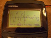
- a simulation - 20KHz sine wave sampled at 44.1KHz and unfiltered,
- hand held scope's response to an analogue 20KHz square wave showing its limitations,
- ECC88 feedback preamp's output response to a 16/44.1K 20KHz sine WAV file input to DAC,
- EF80/transformer preamp's output response to a 16/44.1K 20KHz sine WAV file input to DAC.
Of course, there's the other problem with NOS, created by the finite hold period at the low 44.1KHz sample frequency which becomes relatively more significant for high signal frequencies, causing a sin(x)/x roll-off of ~3dB at 20KHz, but I haven't corrected for this.
Attachments
- Status
- This old topic is closed. If you want to reopen this topic, contact a moderator using the "Report Post" button.
- Home
- Source & Line
- Digital Line Level
- AD1865 DAC valve amp