The clock select is in the firmware, sent out by I2C as well as some other nice features. You may tap it "as is" from ENA pin of oscillators which are there too although they may not shut one of 'em down...
The tricky part of it is to use the connector as is, without extra hacking, as the hacking thing turns the project into ugly nest of wires and PCB cuts - i don't like it...
Or just drop the anamero and go with CM, they are cheaper, available and seems okay for the task, yet their clocks seem a bit on the high side /50M?! cmon, it's audio!/
"less of 50ohm" (source termination) is taken of sum of source impedance of IC driving the line + this resistor = characteristic impedance of the line.
End terminating resistors should be equal to transmission line impedance, so no 22ohms are allowed there.
Last edited:
I have the anamero in front of me, with schematics. There is no manual nor any mention of slaved operation.
Oh, I may write my firmware for cpld, that's interesting! I need to reverse engineer the communication between mcu and cpld first, yet cpld is 32 cell device, should be an easy task. Then I'll be able to implemeent a bit of "drive nos" thing in the board, with extra bit reductions etc.
Sounds like a fun project!
Exactly, hence my question.
My amanero schematic labels its as the 64-cell version, but reverse engineering it should be entirely feasible but I only see a point in that if the MCLK can be pushed down in frequency as the highest you'll ever need with a NOS 1541 is 6.144M, but I find that possibility unlikely as the controller looks to use the mclk rate.
Last edited:
Tazzz, its not documented anywhere, but its there on the board, how else does it select its own clock? the designer has put quite a few extra functions in the firmware editor, i'd say with a bit of ingenuity the clock select signal could be tapped or even sent on the DSDOE pin. ask the designer, I have no need for it so no help from me i'm afraid. he has been forthcoming with some changes and there is definitely undocumented features and control, but no hand holding =)
I would say that way is documented as the schematics are available. But cutting traces and adding wires is much less elegant, I would rather strip it and integrate the controller and the cpld on my own pcb as then it would also be easy to address other issues such as adding a sensible isolation boundary and improving decoupling in the proper way.
BCK divide by 8 for DEM reclock and also feed direct to 1541A??
Hi,
I've here a nice PCB from Mr Rogic with just the TDA1541A section populated, and also one of the OEM M2Tech asynch USB boards. I've been using the two together with good results, and recently removed the isolator (I2S) which improved things further. So why stop now, I'd
like to try Thorstens recommendations listed below from the same thread, and I'm needing some clarification. Any advice is welcome
With 64Fs from the USB device - divide by 8 to have DEM reclocked at 8Fs, which is 352.8kHz at 44.1kHz, 705.6kHz at 88.2kHz.
Ok so far.
The four lines that get re-clocked are WS, DATA, BCK and inverted BCK. The two BCK lines goto DEM at 8Fs, ok.
And the sources Fs64 BCK divided /8 non-inverted signal now feeds the TDA1541A - which is just 352.8kHz at 44.1kHz sampling rate. Is that too low?
Is there any chance that 64Fs wasnt supposed to be divided, only inverted and then fed to the reclocker?. DEM reclock would then be 2.82MHz at 44.1kHz (supposed to work fine) but more to my attention is that BCK to 1541A would also 2.82Mhz - which seems quite normal.
FWIW, I heard the AMR player in Singapore and it was superb. Its based on this, and some others, that I'd happily follow the suggestions listed above.
Regards,
Shane
Hi,
I've here a nice PCB from Mr Rogic with just the TDA1541A section populated, and also one of the OEM M2Tech asynch USB boards. I've been using the two together with good results, and recently removed the isolator (I2S) which improved things further. So why stop now, I'd
like to try Thorstens recommendations listed below from the same thread, and I'm needing some clarification. Any advice is welcome
One of the areas where we can really gain over generica is with DEM reclocking and I2S Attenuators. For this my recommendation would be to use the classic, simple passive I2S attenuators and direct resistive DEM reclocking John Brown (ecdesigns) kindly shared with the diya community.
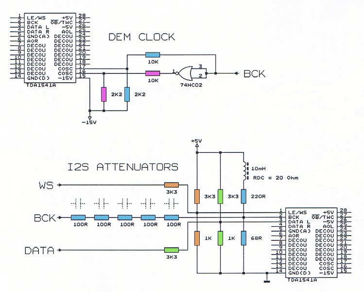
For simplicity, use a 74HC4040 to divide BCK (which will be between 32 and 64Fs depending on your precise source) down for the DEM reclocker so you get between 4 and 8 Fs for the reclock, other frequencies do work, but can be tricky to get to work reliably, let's walk before we run.
With 64Fs from the USB device - divide by 8 to have DEM reclocked at 8Fs, which is 352.8kHz at 44.1kHz, 705.6kHz at 88.2kHz.
Ok so far.
In front of the I2S attenuator place a reclocker.
So I would use a multi-flipflop reclocker instead, a 74HC175 is a quad, allowing us also to reclock the divided down BCK for the DEM reclocking. So the 74HC4040 is connected from the BCK in front of the re-clocker.
With the 74HC175 we have both inverted and non-inverted outputs, so we can drive the DEM reclocker directly, no extra inverters needed. As the I2S attenuator circuit will pose a load onto the reclocker IC (and through it on the supply) it is best to add the same components to the unused output, where they balance the load, so we do not see any PSU load change if the outputs change state.
The four lines that get re-clocked are WS, DATA, BCK and inverted BCK. The two BCK lines goto DEM at 8Fs, ok.
And the sources Fs64 BCK divided /8 non-inverted signal now feeds the TDA1541A - which is just 352.8kHz at 44.1kHz sampling rate. Is that too low?
Is there any chance that 64Fs wasnt supposed to be divided, only inverted and then fed to the reclocker?. DEM reclock would then be 2.82MHz at 44.1kHz (supposed to work fine) but more to my attention is that BCK to 1541A would also 2.82Mhz - which seems quite normal.
IC use is modest, just a 74HC175 reclocker and a 74HC4040 as divider for the DEM Clock in front of the TDA1541.
Having now all and sundry clocks, data etc. entering the TDA1541 marching in German Wehrmacht Lockstep, at reasonably close to optimum levels for the TDA1541 internal logic as well, we can move on.
Ciao T
FWIW, I heard the AMR player in Singapore and it was superb. Its based on this, and some others, that I'd happily follow the suggestions listed above.
Regards,
Shane
The four lines that get re-clocked are WS, DATA, BCK and inverted BCK. The two BCK lines goto DEM at 8Fs, ok.
And the sources Fs64 BCK divided /8 non-inverted signal now feeds the TDA1541A - which is just 352.8kHz at 44.1kHz sampling rate. Is that too low?
Is there any chance that 64Fs wasnt supposed to be divided, only inverted and then fed to the reclocker?. DEM reclock would then be 2.82MHz at 44.1kHz (supposed to work fine) but more to my attention is that BCK to 1541A would also 2.82Mhz - which seems quite normal.
I recently completed my 'veroboard' dac implemently as many of Thorsten's hints and recommendations that I could find.
With the reclocking, I fed the 74HC4040 with BCK directly from my USB/I2S converter (WaveIO), divided it by four, and then sent that to the 74HC175. The 74HC175 then outputs the reclocked BCK/4 and inverted BCK/4 to the TDA1541a dem circuit.
The 74HC175 is therefore fed WS, DATA, BCK, and BCK/4 and outputs reclocked WS, DATA, BCK, BCK/4, and inverted BCK/4 to the dac chip. You can also try other frequencies for DEM reclocking as suggested by Thorsten by choosing different outputs of the 74HC4040. BCK/4 works for my dac, but I have not tried higher frequencies.
Another thing to note that I have discovered in my research is that if you reclock synchronously, only one flip flop is needed but if you reclock asynchronously, it is recommended that the signals are reclocked with two flip flops in series, for reasons of metastability. On my dac I am reclocking asynchonously since I did not want to use MCK from my WaveIO after it passed through the I2S isolator, so I added another 74HC175 after the fact by piggy backing onto the first 74HC175 (not pin for pin, some wiring needed), and reclocking with a 12MHz Tent clock that is on a DDDAC USB/I2S receiver that I no longer use.
I also found out that the 74HC175 has a maximum operating frequency of about 30 to 35 MHz, depending on Vcc. So if you are contemplating reclocking with a high frequency clock, the 74VHC175 is the better flip flop to use. I will probably do that in the future and try reclocking with a 100 MHz clock.
My experience with I2S isolation appears to be different from yours. I started out with no isolation and found ground noise at approximately 180 kHz and 0.5 volt on the dac ground. The noise was traced to my USB hard drive power supply. I then implemented the I2S isolation on the WaveIO and the biggest difference soundwise was a huge reduction in high frequency harshness. The 180 kHz was also no longer present on the dac ground.
With the reclocking, I fed the 74HC4040 with BCK directly from my USB/I2S converter (WaveIO), divided it by four, and then sent that to the 74HC175. The 74HC175 then outputs the reclocked BCK/4 and inverted BCK/4 to the TDA1541a dem circuit.
The 74HC175 is therefore fed WS, DATA, BCK, and BCK/4 and outputs reclocked WS, DATA, BCK, BCK/4, and inverted BCK/4 to the dac chip. You can also try other frequencies for DEM reclocking as suggested by Thorsten by choosing different outputs of the 74HC4040. BCK/4 works for my dac, but I have not tried higher frequencies.
Thanks for this..
With the 74HC175 I take it that Q with a line above it represents the inverted output for any given input, and therefore can see now how you get 5 outputs from something that has 4 inputs.
Can you think of any issues with using 74HC4040 for BCK/8?. This would have fDEM at 352.8kHz for 44.1kHz and 705.6kHz with 88.2kHz.
Another thing to note that I have discovered in my research is that if you reclock synchronously, only one flip flop is needed but if you reclock asynchronously, it is recommended that the signals are reclocked with two flip flops in series, for reasons of metastability. On my dac I am reclocking asynchonously since I did not want to use MCK from my WaveIO after it passed through the I2S isolator, so I added another 74HC175 after the fact by piggy backing onto the first 74HC175 (not pin for pin, some wiring needed), and reclocking with a 12MHz Tent clock that is on a DDDAC USB/I2S receiver that I no longer use.
Interesting that I have the same spare Clock here. How would you expect the performance of the Tent Clock to be compared with the newer units (MEC etc) found on decent USB to I2S converters?
Is there a problem using a clock who's frequency is not a direct multiple of the sampling frequency? ie. 22.5792MHz MCK = 512 x 44.1kHz, 12MHz is 272.11 x 44.1kHz.
IIRC Thorsten mentioned "the clock in the source should have a very good fully seperated supply", is it safe to assume that he was using MCK from the source device as the clock for the re-clocking circuit?
Where he says "As the I2S attenuator circuit will pose a load onto the reclocker IC (and through it on the supply) it is best to add the same components to the unused output, where they balance the load, so we do not see any PSU load change if the outputs change state.
Which unused output is he referring to here? - The only unused outputs on the reclocker are the inverted WS, DATA and BCK. I guess it must be those.
If this is the case, is he's just biasing up these outputs to the same level as the uninverted ones that go to the 1541A, using a duplicate of the resistor divider in the attenuator circuit, or is he actually loading them down somehow, using the same series resistors and some shunt element which repesents the load of the 1541A's inputs (or both?)?
I also found out that the 74HC175 has a maximum operating frequency of about 30 to 35 MHz, depending on Vcc. So if you are contemplating reclocking with a high frequency clock, the 74VHC175 is the better flip flop to use. I will probably do that in the future and try reclocking with a 100 MHz clock.
I'd noticed the CD74HC175 had a maximum of 25MHz, I'll look for the VHC version as you mention. The 74HC4040 looks to be ok with a max frequency typically 45Mhz, and minimally (for a maximum) 29MHz.
My experience with I2S isolation appears to be different from yours. I started out with no isolation and found ground noise at approximately 180 kHz and 0.5 volt on the dac ground. The noise was traced to my USB hard drive power supply. I then implemented the I2S isolation on the WaveIO and the biggest difference soundwise was a huge reduction in high frequency harshness. The 180 kHz was also no longer present on the dac ground.
It seems that way. The reasons for it are however beyond my understanding at this point.
Would you happen to have a schematic of how you've implemented your solution, or at least how to connect up the 74HC4040, 74HC175 (what to do with CLR and MR respectively) etc etc.
Thanks,
Shane
Thanks for this..
Yes.With the 74HC175 I take it that Q with a line above it represents the inverted output for any given input, and therefore can see now how you get 5 outputs from something that has 4 inputs.
I will try to answer the rest of your questions to the best of my ability but please understand that I am just a diy guy who has spent many hours researching the internet and trying to figure out in my mind the ins and outs of building a TDA1541a dac. I have no electrical engineering or electrical design training. So if anyone finds any mistakes in my answers, please chime in.
Both Thorsten and John of ecdesigns have indicated that lower frequencies have higher probabilities of success. The thread Building the ultimate NOS DAC using TDA1541A has information on this and on other aspects of the TDA1541a.Can you think of any issues with using 74HC4040 for BCK/8?. This would have fDEM at 352.8kHz for 44.1kHz and 705.6kHz with 88.2kHz.
The Tent clock is supposed to be very good. I am not familiar with the MEC clock. I will probably buy a Crystek CCHD-950-25 clock oscillator when I upgrade.Interesting that I have the same spare Clock here. How would you expect the performance of the Tent Clock to be compared with the newer units (MEC etc) found on decent USB to I2S converters?
That is asynchronous reclocking and when the clock frequency is an exact multiple of the sampling frequency, it is synchronous reclocking.Is there a problem using a clock who's frequency is not a direct multiple of the sampling frequency? ie. 22.5792MHz MCK = 512 x 44.1kHz, 12MHz is 272.11 x 44.1kHz.
My understanding is that as long as you reclock with two flip flops in series, asynchronous reclocking is not a problem. I did asychronous reclock with only one flip flop for a while and the only issue is that I would hear a very quiet "click" once in a while. It wasn't too noticeable but I did add another flip flop. With synchronous reclocking, only one flip flop is required.
I assume so. Before I implemented the I2S isolator on my WaveIO, I was using its MCK for reclocking. Because I have a very good power supply for the WaveIO, I did not try to hack up the WaveIO to install a separate supply to the clock. Now that I am using the Tent clock on the DDDAC board, I am powering it with the pre-regulator supply for the 74HC chips. The DDDAC board has regulators so I did not provide additional regulation.IIRC Thorsten mentioned "the clock in the source should have a very good fully seperated supply", is it safe to assume that he was using MCK from the source device as the clock for the re-clocking circuit?
Yes, I believe he is referring to the unused inverted outputs of the 74HC175.Where he says "As the I2S attenuator circuit will pose a load onto the reclocker IC (and through it on the supply) it is best to add the same components to the unused output, where they balance the load, so we do not see any PSU load change if the outputs change state.
Which unused output is he referring to here? - The only unused outputs on the reclocker are the inverted WS, DATA and BCK. I guess it must be those.
I just loaded the outputs with the same resistors as the attenuator circuit. This is probably not 100 percent correct as it does not take the impedance of the TDA1541a circuits into consideration but I figure it is better than not doing anything.If this is the case, is he's just biasing up these outputs to the same level as the uninverted ones that go to the 1541A, using a duplicate of the resistor divider in the attenuator circuit, or is he actually loading them down somehow, using the same series resistors and some shunt element which repesents the load of the 1541A's inputs (or both?)?
The 74VHC174 is only necessary if you intend to reclock with a clock frequency that is higher than the chip's maximum operating frequency.I'd noticed the CD74HC175 had a maximum of 25MHz, I'll look for the VHC version as you mention. The 74HC4040 looks to be ok with a max frequency typically 45Mhz, and minimally (for a maximum) 29MHz.
It seems that way. The reasons for it are however beyond my understanding at this point.
I don't have a schematic. For the 74HC175, the I2S lines go to the inputs, the outputs go to the I2S attenuators, the divided BCK and inverted divided BCK output go to the DEM reclock (no 74HC02 required). Unused inverted outputs with resistors to digital ground. Power (+5 volts) to Vcc and CLR, GND to digital ground.Would you happen to have a schematic of how you've implemented your solution, or at least how to connect up the 74HC4040, 74HC175 (what to do with CLR and MR respectively) etc etc.
For the 74HC4040, BCK from USB/I2S to input, your choice of output to 74HC175 input, power to Vcc, RESET and GND to digital ground.
The mening of "synchronous" is that the clocks have a fixed phase relation possibly with a integer division so just having two clocks with the same frequency does not guarantee they being in phase
Asynchronous reclocking ads copious amounts of random jitter but as long as it does not have a relation to the data being converted it transfers to the analog domain as a degraded noisefloor.
Asynchronous reclocking ads copious amounts of random jitter but as long as it does not have a relation to the data being converted it transfers to the analog domain as a degraded noisefloor.
Thanks, Ben.
All of that makes good sense, and if a lower frequency for DEM is a better place to start, then 64Fs BCK divide by 8 is what I'll try first.
The only question I have, how to set 74HC4040 to divide by 8?.
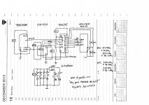
Here is what I plan to try once I know how to set the divider up. Hopefully it resembles accurately everything that has been suggested.
As always, any comments are welcome.
**edit - 74HC4040 CLK is supposed to be BCK and not MCK from the USB > I2S device as drawn.
Regards,
Shane
All of that makes good sense, and if a lower frequency for DEM is a better place to start, then 64Fs BCK divide by 8 is what I'll try first.
The only question I have, how to set 74HC4040 to divide by 8?.
Here is what I plan to try once I know how to set the divider up. Hopefully it resembles accurately everything that has been suggested.
As always, any comments are welcome.
**edit - 74HC4040 CLK is supposed to be BCK and not MCK from the USB > I2S device as drawn.
Regards,
Shane
Attachments
Last edited:
Thanks, Ben.
The only question I have, how to set 74HC4040 to divide by 8?.
Here is what I plan to try once I know how to set the divider up. Hopefully it resembles accurately everything that has been suggested.
As always, any comments are welcome.
**edit - 74HC4040 CLK is supposed to be BCK and not MCK from the USB > I2S device as drawn.
Regards,
Shane
For the 74HC4040, Q1 is /2, Q2 is /4, Q3 is /8, etc.
Looking at your schematic, I treated the unused inverted outputs of the 74HC175 differently. Instead of sending the outputs to the voltage divider circuit as you have shown, I connected the outputs to inline resistors of the same value as the non-inverted outputs and then to digital ground. As I mentioned previously, this does not take into consideration for the TDA1541a circuitry impedances. I suppose measurements of the current in the inline resistors of the I2S lines could be done by measuring the voltage drop across a resistor in each line to determine the current and then adjust the resistors in the inverted outputs to match the corresponding non-inverted currents. It's a fine tuning thing I think, and I have not done that to my dac (I'm not even sure if what I suggested will work). So the current demand on the inverted outputs may be different than on the non-inverted outputs of the 74HC175 in my dac, but it's probably no worse than not loading the unused outputs at all, and hopefully better.
Thanks again.
Using your idea to measure volt drop across the series R to get a value for load currents, if we then bias the unused outputs to the same voltage level (so 1.2V for 1/DATA, 1/WS and 1.2V for 1/BCK), a value of resistance to ground can be selected, which would have the unused outputs at the same voltage potential and with the same load currents as the used outputs.
Do you think there is any switching noise associated with these unused outputs that we dont want going to digital ground?. I note he has the inductor in the BCK voltage divider to stop something along these lines getting back into the 5V supply. It might be worth doing the same with the series resistor from 1/BCK to ground?
**(edit) 1.1V for 1/BCK
Regards,
shane
Last edited:
Thanks again.
Do you think there is any switching noise associated with these unused outputs that we dont want going to digital ground?. I note he has the inductor in the BCK voltage divider to stop something along these lines getting back into the 5V supply. It might be worth doing the same with the series resistor from 1/BCK to ground?
**(edit) 1.1V for 1/BCK
I really don't know if switching noise would be an issue or not. What is definitely important is paying attention to the return paths. What I have done on my dac is keep the paths from inverted outputs to ground of the chip as short and as direct as possible.
Thorsten and others have emphasized the importance of paying attention to supply loops and signal loops, to keep them small and to keep them from crossing or overlapping. His and other people's advice on locations of power supplies relative to signal paths, and placement of chips etc. to minimise sizes of supply loops and signal loops should be followed.
")
PCBs
I am extremely interested in your TDA1541A PCB board along with the Thorsten's tube stage board. Have you finished the designed stage and have the PCBs? What are the prices?
Also, at what point you are joining the digital ground to analog ground? I vaguely remember Thorsten recommended to keep two grounds separate and only joining them at one point, i.e. under pin 5.
Here is one based on Thorsten's 2005 schematic. The inductors are panasonic with mu metal shields. To save board space, output capacitors are external of the board.
I am extremely interested in your TDA1541A PCB board along with the Thorsten's tube stage board. Have you finished the designed stage and have the PCBs? What are the prices?
Also, at what point you are joining the digital ground to analog ground? I vaguely remember Thorsten recommended to keep two grounds separate and only joining them at one point, i.e. under pin 5.
- Status
- This old topic is closed. If you want to reopen this topic, contact a moderator using the "Report Post" button.
- Home
- Source & Line
- Digital Line Level
- Any good TDA1541A DAC kit?