Hi,
At a guess, either wrong value, wrong capacitor type, ground routing issues...
In a differential system you should have one capacitor across +/- out and one each from each output to ground.
If this "coke" is a 4-terminal device and operates on differential outputs then it is not a "choke" in the traditional sense.
The problem with a choke following an I-Out DAC is that the DAC's voltage compliance (real or datasheet) will be massively exceeded... Luckily enough with the Philips parts and common mode only chokes this not much of an issue.
Ciao T
I flirted with cap to ground but didn't much like the sound on TDA1543 or TDA1545.
At a guess, either wrong value, wrong capacitor type, ground routing issues...
In a differential system you should have one capacitor across +/- out and one each from each output to ground.
The series inductor I chose was one with a high SRF (above 200MHz) intended for use as a CM choke.
If this "coke" is a 4-terminal device and operates on differential outputs then it is not a "choke" in the traditional sense.
The problem with a choke following an I-Out DAC is that the DAC's voltage compliance (real or datasheet) will be massively exceeded... Luckily enough with the Philips parts and common mode only chokes this not much of an issue.
Ciao T
Last edited:
At a guess, either wrong value, wrong capacitor type, ground routing issues...
Yep, all issues considered and looked into at the time.
In a differential system you should have one capacitor caross +/- out and one each from each output to ground.
I generally dispense with caps to gnd (Y) in such and just keep the one X-type.
If this "coke" is a 4-terminal device and operates on differential outputs then it is not a "choke" in the traditional sense.
Yes and no - it has appreciable leakage inductance.
The problem with a choke following an I-Out DAC is that the DAC's voltage compliance (real or datasheet) will be massively exceeded... Luckily enough with the Philips parts and common mode only chokes this not much of an issue.
Yep - this is not a configuration I've been tempted to try - choke straight after I-out DAC.
s3tup said:What about my grounds layout?
I didn't liked the capacitive/inductive coupling of DGND and AGND when they are on top of each other (2-layers), so i decided to move the DGND aside.
By doing this i halved the AGND impedance, got solid AGND layer
But i've got a half-circle loop between -5V and DGND pins with -5V PSU in between. The DAC chip is in center of EMI field produced by currents flowing from -5 to DGND and back given the "right hand rule" is true.
My latest layout (not yet built) also has the ground plane for the digital section next to the analog ground plane on the same layer. The tda is on the edge of the Agnd plane (though completely on that plane), and the dgnd plane connects on the entire left side of the tda to the agnd plane. Both planes are almost not interrupted.
One of my previous layouts had dgnd and agnd connect at the agnd pin of the tda only... Worked quite well.
Ecdesigns has, in his latest versions, completely abandoned this discussion: he uses one big ground plane now!
gaetan8888 said:I've take a look today at the Stereophile web site and I can't find those tests.
Can you tell me, please, where they are in the Stereophile web site ?
They are in the March issue (print).
This review will be posted in the free on-line archives at Home Page | Stereophile.com next Thursday or Friday.
John Atkinson
Editor, Stereophile
Damn i've gone thru 5 layouts, and still think i should scrap the current layout and redo it from EMC point of view /since i discovered EMC Information Centre - The EMC Journal (Free in the UK) .
"Balanced" PSU is BS, you need every cap stuck into low impedance ground to work, otherwise it will just pass the spike from V+ to "GND" without any filtering.
I2S wires should be done without DIP sockets to prevent EMC emissions due to impedance mismatch.
"I2S attenuator" should be done in 2 parts, with loading resistors near DAC and series resistors near DF.
Rethink the GND cutouts from "slot antenna" perspective.
And overall layout of connections/wires when the board goes into real-world application.
Ferrite beads and common mode chokes should be placed everywhere, at least on the points of I/O connections on the board, to prevent EMI emissions/fishing.
Every current should be returned to it's source, otherwise it will find it's way back thru air/other circuit paths affecting the performance of DAC surrounding.
Common ground for D and A sides of DAC is reasonable in many ways. Less EMC due to solid ground, the D and A parts of 1541 are probably capacitively coupled much better than our GND impedance. Therefore, the more impedance we add to GND pins, the less current the GND will catch, and more A to D interference will be there.
GND layers should expand to PCB edges, much futher than other wires, so GND could catch and return emitted EM fields.
Every EM transmitter is a receiver too, in same frequencies and same power, therefore, fighting EM emissions reward us with lower EM fishing too.
I know i'll end-up with solid single GND, and PSU layed-out on one side of the board
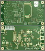
I picked up a red barron PCB 'cause I won't have time to build a PCB for a while.
I was planning on using SMD caps for decoupling by grinding the solder mask off the top layer ground plain. Then I saw that the i-outs are routed right under the TDA1541 cutting the groundplain in half.
I am thinking of removing the mask off that area under theath completely and soldering a thick piece of coper foil underneath the TDA. Going to be a PITA.
An externally hosted image should be here but it was not working when we last tested it.
Last edited:
Hi,
Go for it.
Or just use my suggested Veroboard method. If you have enough silverfoil you can even make an all silver DAC that way...
Ciao T
I picked up a red barron PCB 'cause I won't have time to build a PCB for a while.
I was planning on using SMD caps for decoupling by grinding the solder mask off the top layer ground plain. Then I saw that the i-outs are routed right under the TDA1541 cutting the groundplain in half.
I am thinking of removing the mask off that area under theath completely and soldering a thick piece of coper foil underneath the TDA.
Go for it.
Or just use my suggested Veroboard method. If you have enough silverfoil you can even make an all silver DAC that way...
Ciao T
This review will be posted in the free on-line archives at Home Page | Stereophile.com next Thursday or Friday.
John Atkinson
Editor, Stereophile
Hello
Thank you Mr Atkinson
Are you going to the Montreal Hi-Fi Show (Salon Son & Image) this year ?
Bye
Gaetan
 OT posts and insults removed. Warnings given. Keep it civil, gentleman.
This one goes to production tomorrow, unless i'll find something to fix at mornin' coffee.
- Added some ferrite beads on power rails
- A bit of cutouts around PS ferrites to lower parasitic capacitance around 'em.
- Changed reg bypass caps to electrolytics, as LM317/337 have no love for low impedance on their outputs, but they want some caps to stay stable.
- Some graphics added.
- AGND/DGND could be stitched together with a bit of solder around plane edges.
- Pad for foil-screen grounding. You can glue a ribbon of foil around 1541, and solder it to the pad. Aaargh, DGND or AGND?! Okay, ive added the same "pad" on DGND side too. /not in pic/
- A tiny pad for I2S att resistors, pretty optional, as i had no place to mount them in a good way, and i didn't want to pass traces under resistor's belly due to parasitic capacitance. The resistors could be mounted on their side, between I2S pins and a spot on DGND.
Attachments
Last edited:
Hi,
Have fun.
However you realise that you have more suboptimal design features than I can cover in one post?
Have you actually read the the thread and those referenced within?
What you have will work about as well as what Philips and Marantz did in their 1980's CD-Players.
Ciao T
This one goes to production tomorrow
Have fun.
However you realise that you have more suboptimal design features than I can cover in one post?
Have you actually read the the thread and those referenced within?
What you have will work about as well as what Philips and Marantz did in their 1980's CD-Players.
Ciao T
One post (well two) from Guido elsewhere:
part 1 power supply
digital part: all logic is current mode (constant current).
most of the supply +5 to -5, lesser part +5 to dgnd.
Capacitive spike to -15V.
analog part: -15: current reference generator, dem oscillator and
ring-counter. Not to agnd, but to -5. :!:
This 10V should be as constant as possible.
Decouple all supply pins and DEM caps to agnd.
Logic before dac (e.g. for reclocking) and the caps to filter the i2s inputs (see i2s chapter) also to dgnd.
agnd - dgnd should then only be some dc current.
part2: i2s inputs
Reclocking needed on ALL inputs (to avoid disturbance due to jitter on the inputs). Output latch is clocked on BCK pulse in i2s mode (1541A).
input voltages low 1.3 min (1.2 for safety) and high 1.5V max (1.6 for safety). So instead of 'TTL levels' 1.2 and 1.6V.
Rise time not faster than 10nsec, reduce speed with 10pF cap to dgnd (RC filter: 1k resistor and 10pF cap). Drive this RC filter in such a way that 1.2 for low and 1.5 for high goes to the dac.
Thorsten,
Do you refer to lack of:
- DEM clocking,
- I2S attenuation
- I2S reclocking
- Shunt regs
I'm well aware of these. I2S things will be on digital board, shunt regs is a matter of choice, and DEM clocking - i'll try without it.
Or there are more suboptimal design features?
Regal, these suggestions are from HtP, he is somehow related to Phillips:
http://www.diyaudio.com/forums/digital-line-level/31780-tda1541-info-6.html
Nice read...
Last edited:
Regal, these suggestions are from HtP, he is somehow related to Phillips:
http://www.diyaudio.com/forums/digital-line-level/31780-tda1541-info-6.html
Nice read...
So you see that there should be a cap from -15V to -5V (close to the chip), so the internal 10V reference is as good as possible ?
Hi,
Non of the above.
If you do not use any proper re-clocking and no DEM re-clocking and no I2S attenuators or shunt regulators, this is a choice, though it is severely suboptimal in itself.
I am referring to the power supply arrangements (as there is little else on the board) where you reserve the worst regulator for the moist sensitive voltage and your valiant attempt to maximise jitter resulting from the interconnection between source (Digital Filter) and DAC Chip.
Really. And you REALLY think this is a good idea? Especially with a ribbon cable connection to the TDA1541 and the impedances involved?
Of course there many ways skinning digital cat's. I just see in your design about all the various ways in which to get thing wrong faithfully implemented and what may seem a deliberate rejection of all the good information available about how the TDA1541 works, about how digital connections with known impedance connections can be optimised, etc., et al.
Anyway, you have fun your way.
However, do me one favour. If you find the results of your efforts to be less than good at delivering the sound quality you expect, do not blame the TDA1541, but the designer.
Ciao T
Thorsten,
Do you refer to lack of:
- DEM clocking,
- I2S attenuation
- I2S reclocking
- Shunt regs
Non of the above.
If you do not use any proper re-clocking and no DEM re-clocking and no I2S attenuators or shunt regulators, this is a choice, though it is severely suboptimal in itself.
I am referring to the power supply arrangements (as there is little else on the board) where you reserve the worst regulator for the moist sensitive voltage and your valiant attempt to maximise jitter resulting from the interconnection between source (Digital Filter) and DAC Chip.
I'm well aware of these. I2S things will be on digital board
Really. And you REALLY think this is a good idea? Especially with a ribbon cable connection to the TDA1541 and the impedances involved?
Of course there many ways skinning digital cat's. I just see in your design about all the various ways in which to get thing wrong faithfully implemented and what may seem a deliberate rejection of all the good information available about how the TDA1541 works, about how digital connections with known impedance connections can be optimised, etc., et al.
Anyway, you have fun your way.
However, do me one favour. If you find the results of your efforts to be less than good at delivering the sound quality you expect, do not blame the TDA1541, but the designer.
Ciao T
Hi,
If the cable is short enough it's characteristic impedance will not matter.
How much is "short enough", depends on a LOT of factors, mostly risetime.
In general I would suggest not running digital audio through those kind of cables without taking care of impedance matching and other factors.
Ciao T
I'm not getting the ribbon cable comment, I've seen a lot of higher end DAC (albeit not tda1541) where the input section is a separate board with small (1") jumpers connecting I2S to the main board. Is impedance mismatch an issue with a tiny jumper?
If the cable is short enough it's characteristic impedance will not matter.
How much is "short enough", depends on a LOT of factors, mostly risetime.
In general I would suggest not running digital audio through those kind of cables without taking care of impedance matching and other factors.
Ciao T
Thorsten, thanks for constructive critics! That's what i'm looking for when i post some PCBs/etc.
I hate "i won't comment 'coz i don't want to be mean on poor silly DIYer for his work".
Rough, plain comments are welcome! As long as they are constructive...
I wrote severeal different posts but decided to delete em. They weren't constructive, and were theorized too much Hands-on is the best.
I'll make veroboard rig with current-sense resistors everywhere to investigate 1541 behaviour.
I know i won't get nice THD plots, but at least i'll know where the current flows, it's shape, and what affects it.
I hate "i won't comment 'coz i don't want to be mean on poor silly DIYer for his work".
Rough, plain comments are welcome!
As long as they are constructive...I wrote severeal different posts but decided to delete em. They weren't constructive, and were theorized too much
Hands-on is the best.I'll make veroboard rig with current-sense resistors everywhere to investigate 1541 behaviour.
I know i won't get nice THD plots, but at least i'll know where the current flows, it's shape, and what affects it.
Hi,
Excellent. I did that once as well. It is important to know where current flows.
There are articles that cover most of the TDA1541 internals. Personally I have some papers (over 100 pages) that originally where Philips internal and go into even bigger detail, but they are in storage and I never scanned them.
The other part is pretty common sense. I would use a re-clocker close to the DAC (ANY DAC, not just 1541) and make sure the only current flowing in the digital ground plane between DAC and reclocker are the return currents of the signal (no supply currents etc.).
Reclockers themselves can have a fair bit of ground bounce which needs to be considered. If the MCK/Reclock Clock cannot be local I would look seriously at how we transmit it and what loading we have on the line.
PERSONALLY I would use 75R Micro Coax with correct connectors for the clock and make sure to back terminate it (if necessary use a discrete clock driver on the sending side) if it is on a separate PCB.
If having the clock on the same PCB look at rise times and consider a back-terminated strip-line.
The "big deal" with the reclocker is that gives you much more control over the whole affairs and allows you to get the jitter at the DAC to be VERY CLOSE to that of your clock.
Now if your clock is horrible bad it will not help, but if you have significant distance between source and maybe poorly terminated ribbon cables with a decent clock (say a Wolfson Micro Receiver well implemented) it can make a big difference...
BTW, I would seriously sync DEM clock and wordclock at integer multiples of four or more for the DEM Clock to wordclock ratio.
As I pointed out earlier, using the re-clocker I suggested (74...175) offers differential outputs, which incidentally can help with the ground bounce if loaded equally, so dealing with the DEM reclocking becomes easy...
Ciao T
I'll make veroboard rig with current-sense resistors everywhere to investigate 1541 behaviour. I know i won't get nice THD plots, but at least i'll know where the current flows, it's shape, and what affects it.
Excellent. I did that once as well. It is important to know where current flows.
There are articles that cover most of the TDA1541 internals. Personally I have some papers (over 100 pages) that originally where Philips internal and go into even bigger detail, but they are in storage and I never scanned them.
The other part is pretty common sense. I would use a re-clocker close to the DAC (ANY DAC, not just 1541) and make sure the only current flowing in the digital ground plane between DAC and reclocker are the return currents of the signal (no supply currents etc.).
Reclockers themselves can have a fair bit of ground bounce which needs to be considered. If the MCK/Reclock Clock cannot be local I would look seriously at how we transmit it and what loading we have on the line.
PERSONALLY I would use 75R Micro Coax with correct connectors for the clock and make sure to back terminate it (if necessary use a discrete clock driver on the sending side) if it is on a separate PCB.
If having the clock on the same PCB look at rise times and consider a back-terminated strip-line.
The "big deal" with the reclocker is that gives you much more control over the whole affairs and allows you to get the jitter at the DAC to be VERY CLOSE to that of your clock.
Now if your clock is horrible bad it will not help, but if you have significant distance between source and maybe poorly terminated ribbon cables with a decent clock (say a Wolfson Micro Receiver well implemented) it can make a big difference...
BTW, I would seriously sync DEM clock and wordclock at integer multiples of four or more for the DEM Clock to wordclock ratio.
As I pointed out earlier, using the re-clocker I suggested (74...175) offers differential outputs, which incidentally can help with the ground bounce if loaded equally, so dealing with the DEM reclocking becomes easy...
Ciao T
Are you going to the Montreal Hi-Fi Show (Salon Son & Image) this year ?
Sadly, no. But Robert Deutsch and Art Dudley will be representing Stereophile at the 2012 SSI and reporting live.
John Atkinson
Editor, Stereophile
- Status
- This old topic is closed. If you want to reopen this topic, contact a moderator using the "Report Post" button.
- Home
- Source & Line
- Digital Line Level
- Any good TDA1541A DAC kit?