Hello !
I have made a non-OS dac with a TDA1545, featuring an innovative IV stage and jitter reduction techniques. Have a look :
http://peufeu.free.fr/audio/extremist_dac/
Any comments are appreciated")
Regards
Pierre
I have made a non-OS dac with a TDA1545, featuring an innovative IV stage and jitter reduction techniques. Have a look :
http://peufeu.free.fr/audio/extremist_dac/
Any comments are appreciated
Regards
Pierre
It was about year ago…
http://pub134.ezboard.com/ffakeidsfrm1.showMessage?index=62&topicID=237.topic
I was patient, didn’t I?
Pedja
http://pub134.ezboard.com/ffakeidsfrm1.showMessage?index=62&topicID=237.topic
I was patient, didn’t I?
Pedja
Very good work!
I'm even more impressed by your work on the website. Extremely complete.
http://peufeu.free.fr/audio/ can now be considered as a reference website for DAC builders
I'm even more impressed by your work on the website. Extremely complete.
http://peufeu.free.fr/audio/ can now be considered as a reference website for DAC builders

Hello Pierre, nice site!peufeu said:Hello !
I have made a non-OS dac with a TDA1545, featuring an innovative IV stage and jitter reduction techniques. Have a look :
http://peufeu.free.fr/audio/extremist_dac/
Any comments are appreciated
Regards
Pierre
Also nice design. Interesting I/V stage, very subtle! I still wrestle with the idea that the opamp is not in the signal loop. The opamp has a varying output signal, right? If not, there would be no point to have it in the circuit. Now, this varying output signal can only come from the inverting input signal. So, there IS an input signal. If I understand correctly, the task of the opamp is to keep the DAC output (which is at its inverting input) at zero volts. Suppose the inverting input wants to go pos. This is then corrected by the opamp. The opamp reacts on the error voltage. Looking at it this way, this opamp stage is a normal 100% feedback error loop. Hmm.
Jan Didden
Re: Re: Have a look at my new TDA1545 DAC (lots of details on page)
First, the DAC output voltage must be kept at 3.3V not 0 volts, but that is not important regarding your remark.
Imagine there is no opamp. In that case we would feed the JFET grid from a constant reference voltage, which would be 3.3V + a fixed amount corresponding to the Vgs voltage of this JFET wiht this specific current. Thus, the JFET (acting as a follower) would keep its source at around 3.3V. This has two main drawbacks :
Enter the opamp. Thanks to Feedback, it will apply a correct voltage on the JFET grid to get the right voltage on the DAC output. No more trimming and voltage variations.
Then, how is it out of the signal path ? Simple : the opamp output does not couple to the output signal. Voltage variations on the JFET grid do not transfer to the output signal except through the JFET's internal parasitical capacitance, which is low. Thus, the opamp is out of the signal path...
This is by contrast to the traditional IV using an inverting opamp, where the opamp transmits the full musical signal.
OK ?
janneman said:(snip) ... Looking at it this way, this opamp stage is a normal 100% feedback error loop. Hmm. (snip)
First, the DAC output voltage must be kept at 3.3V not 0 volts, but that is not important regarding your remark.
Imagine there is no opamp. In that case we would feed the JFET grid from a constant reference voltage, which would be 3.3V + a fixed amount corresponding to the Vgs voltage of this JFET wiht this specific current. Thus, the JFET (acting as a follower) would keep its source at around 3.3V. This has two main drawbacks :
- The reference voltage would have to be adjusted according to the specific JFET used (this means a trimpot)
- The source voltage would vary a little with the DAC output current, because the source resistance is not that low.
Enter the opamp. Thanks to Feedback, it will apply a correct voltage on the JFET grid to get the right voltage on the DAC output. No more trimming and voltage variations.
Then, how is it out of the signal path ? Simple : the opamp output does not couple to the output signal. Voltage variations on the JFET grid do not transfer to the output signal except through the JFET's internal parasitical capacitance, which is low. Thus, the opamp is out of the signal path...
This is by contrast to the traditional IV using an inverting opamp, where the opamp transmits the full musical signal.
OK ?
Bricolo said:One thing you could try is the pass labs D1's I/V stage
Isn't this one differential ? I use only one DAC, thus I didn't need a diff stage... I might try a differential DAC in the future maybe...
Hi,
Well, here are some comments:
I am a bit puzzled at the reclocking. The xtal is 11 or 16MHz, depending on the cdp master clock. You are reclocking i2s with that clock.
Does the xtal freq actually have a relation to the i2s clock freq coming in at IC2, or are you just 'reclocking' like the async reclocking designs on the net?? If so, the clock is considered too low speed, think they are using >25MHz.
=====
I dont know the tda1545, but normally data and ws are clocked in when they are stable. Data and ws change at bck going low, so the dac clocks in at bck going high. I did not make timingdiagrams to understand the reclocking circuit, but i hope you did..! Would be nice to see them.
=====
What is wrong in the design in IMHO is that you cannot guarantee that the signals on D4-D6 of IC2 are not changing at the same time as clock on pen 9. This depends on the delay in the loop 'clock to cdp' - cdp decoder/filter - spdif - crystal input chip. There is a small chance this happens, but i guess we both know murphy.. Change the cdp or cable(s) and it might not work anymore..
I am working on a similar dac (for ages...). Also with clockfeedback to cdp. The differences: i am dividing the xtal freq before it goes to the dac (divider adds some jitter, i know) and i am using a FIFO to avoid timing problems.
It is using two tda1541's and a 11MHz clock, since i am using old philips players. Do a search in the dig section.
Greetings,
GuidoB
Re: Re: Re: Have a look at my new TDA1545 DAC (lots of details on page)
Not OK yet, I'm afraid. Look at a traditional I/V with opamp with R between output and invert input. The DAC currents wants to go into the input. That raises the output voltage. Because of the high open loop gain of the opamp, the output voltage rises so much, that almost all of the current of the DAC is absorbed by the output through the R. There only remaines a very low (error) voltage at the inv input to maintain the output level necessary to absorb the DAC current. Because of the limited bandwidth, the opamp gets into trouble by the current steps of the DAC. It will show error voltage pulses at the inv input due to the current steps. This is what you also said.
Now take your circuit. The DAC currents wants to go into the input. That raises the output voltage. Because of the high open loop gain of the opamp, the output voltage rises so much, that almost all of the current of the DAC is absorbed by the FET. There only remaines a very low (error) voltage at the inv input to maintain the output level at the gate necessary for absorbing the DAC current. Because of the limited bandwidth, the opamp gets into trouble by the current steps of the DAC. It will show error voltage pulses at the inv input due to the current steps.
Conclusion: There is no basic difference between a conventional R-feedback I/V and this circuit.
Jan Didden
peufeu said:
First, the DAC output voltage must be kept at 3.3V not 0 volts, but that is not important regarding your remark.
Imagine there is no opamp. In that case we would feed the JFET grid from a constant reference voltage, which would be 3.3V + a fixed amount corresponding to the Vgs voltage of this JFET wiht this specific current. Thus, the JFET (acting as a follower) would keep its source at around 3.3V. This has two main drawbacks :
- The reference voltage would have to be adjusted according to the specific JFET used (this means a trimpot)
- The source voltage would vary a little with the DAC output current, because the source resistance is not that low.
Enter the opamp. Thanks to Feedback, it will apply a correct voltage on the JFET grid to get the right voltage on the DAC output. No more trimming and voltage variations.
Then, how is it out of the signal path ? Simple : the opamp output does not couple to the output signal. Voltage variations on the JFET grid do not transfer to the output signal except through the JFET's internal parasitical capacitance, which is low. Thus, the opamp is out of the signal path...
This is by contrast to the traditional IV using an inverting opamp, where the opamp transmits the full musical signal.
OK ?
Not OK yet, I'm afraid. Look at a traditional I/V with opamp with R between output and invert input. The DAC currents wants to go into the input. That raises the output voltage. Because of the high open loop gain of the opamp, the output voltage rises so much, that almost all of the current of the DAC is absorbed by the output through the R. There only remaines a very low (error) voltage at the inv input to maintain the output level necessary to absorb the DAC current. Because of the limited bandwidth, the opamp gets into trouble by the current steps of the DAC. It will show error voltage pulses at the inv input due to the current steps. This is what you also said.
Now take your circuit. The DAC currents wants to go into the input. That raises the output voltage. Because of the high open loop gain of the opamp, the output voltage rises so much, that almost all of the current of the DAC is absorbed by the FET. There only remaines a very low (error) voltage at the inv input to maintain the output level at the gate necessary for absorbing the DAC current. Because of the limited bandwidth, the opamp gets into trouble by the current steps of the DAC. It will show error voltage pulses at the inv input due to the current steps.
Conclusion: There is no basic difference between a conventional R-feedback I/V and this circuit.
Jan Didden
Re: Re: Re: Re: Have a look at my new TDA1545 DAC (lots of details on page)
Ok, here we go :
On your first paragraph, I'm all OK with you, no problem.
The dilemma with such stages is that you want a high value IV conversion resistor to have a lot of gain, but as the gain increases, the amp may hit slew limiting or go nearer its gain*bandwidth product limits, both things being BAD as they directly affect the music signal.
On to the second paragraph (my IV stage) :
I include a simplified schematic in this post for reference. I removed the cascoding JFET as it has little influence on our argument.
Actually, no. Maybe you have been fooled into thinking this by the way the schematic is drawn. Current likes to go through the path of least impedance. Here, the DAC output current (I_in) can either go through the opamp input or through the JFET source. The JFET source is low impedance (50-100 ohms of dynamic source impedance) thus the current will go through the JFET and through my IV conversion resistor, R1. I'll call "Zs" the source impedance of the JFET.
Now, the current goes through the JFET as if the opamp was not here. But JFETs are bad followers and have higher Zs than bipolars for instance, and J1 would be unable to keep its source voltage fixed when I_In varies. This causes a variation of voltage at the opamp input, which in turn adjusts its output voltage to control the JFET and hold its source voltage at my reference value.
I think your analysis fails to take into account that the JFET is active and will adapt itself to I_in. The opamp just helps it.
Yes indeed, the opamp can go into slew limiting and gain*bw product limiting, but here is the catch :
- The opamp has to control voltage variations on a much smaller impedance than in a traditional IV converter. Here, voltage variations are I_In*Zs whereas in a traditional IV converter these would be I_In*R1. If the JFET has a Zs of 50 Ohms and R1 is 1k, the opamp has a job which is 20 times easier to do (R1/Zs = 20). Therefore we can have our cake and eat it : a lot of gain and no speed problems in our opamp.
- Even if the opamp falls into slew limiting, this does not matter. If the waveform at the output of the opamp is distorted, the voltage at the DAC output WILL vary a little, but only a tiny part of this distorted signal will get into the music signal, because the DAC still has some voltage compliance on its output. By contrast, in the traditional IV stage, all opamp distortion goes into the output signal because the output signal IS the opamp output.
You can think about it by reversing the problem : what would the opamp have to do in order to screw up the signal ? The opamp output can't couple with the output current because almost no current goes into the JFET gate (this is why I did not put a BJT in this position). This leaves the opamp output voltage, which is more or less the DAC output voltage, which must be kept at its reference value. So in order to cause a distortion in the music signal, the opamp would have to distort so badly that it'd cause the DAC output voltage compliance to be exceeded. This is pretty unlikely IMHO.
So this opamp-jfet combo behaves like a "super-jfet" with very low source impedance (ideal for cascoding) at frequencies where the opamp can keep up. But at higher frequencies when the opamp reaches its limits, the JFET still works. So even when the opamp dies, it falls back on the JFET. Graceful degradation.
To be safe I still selected a very fast opamp with good sonics.
Does this make it look clearer ? I hope it helps.
Ok, here we go :
On your first paragraph, I'm all OK with you, no problem.
The dilemma with such stages is that you want a high value IV conversion resistor to have a lot of gain, but as the gain increases, the amp may hit slew limiting or go nearer its gain*bandwidth product limits, both things being BAD as they directly affect the music signal.
On to the second paragraph (my IV stage) :
I include a simplified schematic in this post for reference. I removed the cascoding JFET as it has little influence on our argument.
Now take your circuit. The DAC currents wants to go into the input.
Actually, no. Maybe you have been fooled into thinking this by the way the schematic is drawn. Current likes to go through the path of least impedance. Here, the DAC output current (I_in) can either go through the opamp input or through the JFET source. The JFET source is low impedance (50-100 ohms of dynamic source impedance) thus the current will go through the JFET and through my IV conversion resistor, R1. I'll call "Zs" the source impedance of the JFET.
Now, the current goes through the JFET as if the opamp was not here. But JFETs are bad followers and have higher Zs than bipolars for instance, and J1 would be unable to keep its source voltage fixed when I_In varies. This causes a variation of voltage at the opamp input, which in turn adjusts its output voltage to control the JFET and hold its source voltage at my reference value.
That raises the output voltage. Because of the high open loop gain of the opamp, the output voltage rises so much, that almost all of the current of the DAC is absorbed by the FET. There only remaines a very low (error) voltage at the inv input to maintain the output level at the gate necessary for absorbing the DAC current.
I think your analysis fails to take into account that the JFET is active and will adapt itself to I_in. The opamp just helps it.
Because of the limited bandwidth, the opamp gets into trouble by the current steps of the DAC. It will show error voltage pulses at the inv input due to the current steps.
Yes indeed, the opamp can go into slew limiting and gain*bw product limiting, but here is the catch :
- The opamp has to control voltage variations on a much smaller impedance than in a traditional IV converter. Here, voltage variations are I_In*Zs whereas in a traditional IV converter these would be I_In*R1. If the JFET has a Zs of 50 Ohms and R1 is 1k, the opamp has a job which is 20 times easier to do (R1/Zs = 20). Therefore we can have our cake and eat it : a lot of gain and no speed problems in our opamp.
- Even if the opamp falls into slew limiting, this does not matter. If the waveform at the output of the opamp is distorted, the voltage at the DAC output WILL vary a little, but only a tiny part of this distorted signal will get into the music signal, because the DAC still has some voltage compliance on its output. By contrast, in the traditional IV stage, all opamp distortion goes into the output signal because the output signal IS the opamp output.
You can think about it by reversing the problem : what would the opamp have to do in order to screw up the signal ? The opamp output can't couple with the output current because almost no current goes into the JFET gate (this is why I did not put a BJT in this position). This leaves the opamp output voltage, which is more or less the DAC output voltage, which must be kept at its reference value. So in order to cause a distortion in the music signal, the opamp would have to distort so badly that it'd cause the DAC output voltage compliance to be exceeded. This is pretty unlikely IMHO.
So this opamp-jfet combo behaves like a "super-jfet" with very low source impedance (ideal for cascoding) at frequencies where the opamp can keep up. But at higher frequencies when the opamp reaches its limits, the JFET still works. So even when the opamp dies, it falls back on the JFET. Graceful degradation.
To be safe I still selected a very fast opamp with good sonics.
Does this make it look clearer ? I hope it helps.
Reclocking
Hello Guido !
First of all tanks for your wonderful, so elegant clock modules.
Actually, this CDP (Philips CD723) has a 8.4672MHz clock, so that is the clock frequency that I put in my DAC. Apart from keeping the CDP happy, my DAC poses no condition on clock frequency (read on).
I know my reclocking looks evil. Think about it this way : you want to reclock a signal running at a frequency Fsignal to rid it of jitter (a BCk signal, for instance). For this you use a D latch, fed with a clock of frequency Fclock. The condition for this to work is simply that Fclock = N*Fsignal with N integer and >=2. OK ?
It does not matter if N=2 or 3 or 4 or 50. As long as data setup&hold times are respected, **and jitter does not exceed half a clock cycle**, it will work. For an incoming signal of 50% duty cycle like a bit clock, this is very easy : the triggering clock edge must not coincide with any signal edge, that's all.
If N is odd, the duty cycle of the reclocked signal will change, but this is not the case here (N is even).
What is important is that everything is synchronous here. As I send the clock back to the CDP, it will send a synchronous signal back to the DAC. I checked this. I use the signal decoded by CS8412, and even with all the SPDIF encoding & decoding mess, the bit clock provided by CS8412 stays well in sync with the clock I send to the CDP. Thus this is not asynchronous reclocking. It is well synchronous, because the BCK and the clock always stay aligned.
Should Murphy come around and the CS8412 give me a bit clock that has edges at the wrong places (at the latch sampling points for instance), I would invert the phase of the clock sent to the CDP. Then, everything would be shifted by half a clock period, and there would be no more edge problems.
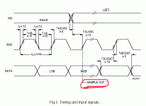
I attached the timing info from the datasheet. Analog sample out and input data acquisition all happen on the BCK rising edge.
Yes, I did some timing diagrams, a long time ago when I designed this thing... I could re-draw and scan them if you really want
You are absolutely right, I was absolutely not sure that it would work when I plugged it in. I had other plans it case it didn't, including FIFOs. That's why I put the SPDIF receiver on a separate board : to be able to change plans if need be.
My design would be quite picky on cables I guess : if the edges fall on the wrong time, boom. But the nice thing is that if it works in a configuration, you can be pretty sure it'll always work. But, remember a half clock cycle at 8.4 MHz makes about 15 meters of propagation distance... This leaves a bit of tolerance.
Anyway, it got me worried, but when I plugged it, it worked, and the waveforms were just like they should be (ie. clock edge right on a stable area of BCK). So I have no more worries now. Seems like Murphy was on vacation.
I think my reclocking features a lot of subtle aerobatics (in the sense of : "hey, this thing works. but I thought this should not work. do I know how it works ? WTF did I put in this thing ?") but I like it this way.
So you divide the clock and send it to the DAC ? Why not ? I think it's a bit more complicated because you have to make sure that this "artificial" BCK agrees with the "real" BCK. You can do this very simply by sending the artificial BCK into the CS8412 receiver. It can be configured so that its BCK is an input. Then, it will output its bits just as you want them.
And, the CS8412 includes a double buffer ! This means it can receive the next sample while sending the current one to your DAC chip. You don't need a FIFO, really. You have one already. I know it looks like it's not going to work unless you put a FIFO, remember I was quite worried. But it just worked. The device stared at me like saying "hey, look, I work. No fuss, man."
Besides, FIFOs are only useful if they are full, but not too full. How do you keep it full enough ? Stop the DAC when it's empty ? Stop the CDP if it fills too much ? When everything is synchronous like here, you don't need a FIFO, you need a double buffer, which is no more than a 2-level FIFO, and which is already included in the CS8412 we all know and love.
So why not take a new look on your project, strip the unneccessary complexity (especially the FIFO) and finally build it ?
Regards !
Pierre
Hello Guido !
First of all tanks for your wonderful, so elegant clock modules.
I am a bit puzzled at the reclocking. The xtal is 11 or 16MHz, depending on the cdp master clock. You are reclocking i2s with that clock.
Actually, this CDP (Philips CD723) has a 8.4672MHz clock, so that is the clock frequency that I put in my DAC. Apart from keeping the CDP happy, my DAC poses no condition on clock frequency (read on).
Does the xtal freq actually have a relation to the i2s clock freq coming in at IC2, or are you just 'reclocking' like the async reclocking designs on the net?? If so, the clock is considered too low speed, think they are using >25MHz.
I know my reclocking looks evil. Think about it this way : you want to reclock a signal running at a frequency Fsignal to rid it of jitter (a BCk signal, for instance). For this you use a D latch, fed with a clock of frequency Fclock. The condition for this to work is simply that Fclock = N*Fsignal with N integer and >=2. OK ?
It does not matter if N=2 or 3 or 4 or 50. As long as data setup&hold times are respected, **and jitter does not exceed half a clock cycle**, it will work. For an incoming signal of 50% duty cycle like a bit clock, this is very easy : the triggering clock edge must not coincide with any signal edge, that's all.
If N is odd, the duty cycle of the reclocked signal will change, but this is not the case here (N is even).
What is important is that everything is synchronous here. As I send the clock back to the CDP, it will send a synchronous signal back to the DAC. I checked this. I use the signal decoded by CS8412, and even with all the SPDIF encoding & decoding mess, the bit clock provided by CS8412 stays well in sync with the clock I send to the CDP. Thus this is not asynchronous reclocking. It is well synchronous, because the BCK and the clock always stay aligned.
Should Murphy come around and the CS8412 give me a bit clock that has edges at the wrong places (at the latch sampling points for instance), I would invert the phase of the clock sent to the CDP. Then, everything would be shifted by half a clock period, and there would be no more edge problems.
I dont know the tda1545, but normally data and ws are clocked in when they are stable. Data and ws change at bck going low, so the dac clocks in at bck going high. I did not make timingdiagrams to understand the reclocking circuit, but i hope you did..! Would be nice to see them.
I attached the timing info from the datasheet. Analog sample out and input data acquisition all happen on the BCK rising edge.
Yes, I did some timing diagrams, a long time ago when I designed this thing... I could re-draw and scan them if you really want
What is wrong in the design in IMHO is that you cannot guarantee that the signals on D4-D6 of IC2 are not changing at the same time as clock on pen 9. This depends on the delay in the loop 'clock to cdp' - cdp decoder/filter - spdif - crystal input chip. There is a small chance this happens, but i guess we both know murphy.. Change the cdp or cable(s) and it might not work anymore..
You are absolutely right, I was absolutely not sure that it would work when I plugged it in. I had other plans it case it didn't, including FIFOs. That's why I put the SPDIF receiver on a separate board : to be able to change plans if need be.
My design would be quite picky on cables I guess : if the edges fall on the wrong time, boom. But the nice thing is that if it works in a configuration, you can be pretty sure it'll always work. But, remember a half clock cycle at 8.4 MHz makes about 15 meters of propagation distance... This leaves a bit of tolerance.
Anyway, it got me worried, but when I plugged it, it worked, and the waveforms were just like they should be (ie. clock edge right on a stable area of BCK). So I have no more worries now. Seems like Murphy was on vacation.
I think my reclocking features a lot of subtle aerobatics (in the sense of : "hey, this thing works. but I thought this should not work. do I know how it works ? WTF did I put in this thing ?") but I like it this way.
I am working on a similar dac (for ages...). Also with clockfeedback to cdp. The differences: i am dividing the xtal freq before it goes to the dac (divider adds some jitter, i know) and i am using a FIFO to avoid timing problems.
So you divide the clock and send it to the DAC ? Why not ? I think it's a bit more complicated because you have to make sure that this "artificial" BCK agrees with the "real" BCK. You can do this very simply by sending the artificial BCK into the CS8412 receiver. It can be configured so that its BCK is an input. Then, it will output its bits just as you want them.
And, the CS8412 includes a double buffer ! This means it can receive the next sample while sending the current one to your DAC chip. You don't need a FIFO, really. You have one already. I know it looks like it's not going to work unless you put a FIFO, remember I was quite worried. But it just worked. The device stared at me like saying "hey, look, I work. No fuss, man."
Besides, FIFOs are only useful if they are full, but not too full. How do you keep it full enough ? Stop the DAC when it's empty ? Stop the CDP if it fills too much ? When everything is synchronous like here, you don't need a FIFO, you need a double buffer, which is no more than a 2-level FIFO, and which is already included in the CS8412 we all know and love.
So why not take a new look on your project, strip the unneccessary complexity (especially the FIFO) and finally build it ?
Regards !
Pierre
Attachments
Re: Reclocking
(I like to repeat myself) :
Problem is : my system fails if clock and BCK have a relative delay which makes the edges mess with each other. I don't know which delay I will have, but I know it is constant. Therefore if my system works once, it will always work.
Anyway, it worked when I plugged it in, and has kept working ever since, for about 1 month of continuous use now.
Ahem
Re: Re: Re: Re: Re: Have a look at my new TDA1545 DAC (lots of details on page)
Yes, it does make it clearer. But observe: the ONLY way that the FET can can change it's source current is when the gate-source voltage varies. It's just built that way. Now, who takes care of the change in gate-source voltage? The opamp, as you say "it helps". Just as it "helps" the resistor in a traditional I/V. And how does the opamp know it has to change the gate voltage? Because it gets an input error voltage. Ergo: there is a direct path from opamp input to gate to source, to output current and thus to output signal. This opamp is in the signal loop, whether you like it or not. Indeed, the FET increases the loop gain and "makes it easier on the opamp". But that was not the point. The point is, is this opamp in the signal loop. I say, you bet.
Jan Didden
peufeu said:Ok, here we go :
[snip]
Here, the DAC output current (I_in) can either go through the opamp input or through the JFET source. The JFET source is low impedance (50-100 ohms of dynamic source impedance) thus the current will go through the JFET and through my IV conversion resistor, R1. I'll call "Zs" the source impedance of the JFET.
Now, the current goes through the JFET as if the opamp was not here. But JFETs are bad followers and have higher Zs than bipolars for instance, and J1 would be unable to keep its source voltage fixed when I_In varies. This causes a variation of voltage at the opamp input, which in turn adjusts its output voltage to control the JFET and hold its source voltage at my reference value.
I think your analysis fails to take into account that the JFET is active and will adapt itself to I_in. The opamp just helps it.
[snip]
- The opamp has to control voltage variations on a much smaller impedance than in a traditional IV converter. Here, voltage variations are I_In*Zs whereas in a traditional IV converter these would be I_In*R1. If the JFET has a Zs of 50 Ohms and R1 is 1k, the opamp has a job which is 20 times easier to do (R1/Zs = 20). Therefore we can have our cake and eat it : a lot of gain and no speed problems in our opamp.
- Even if the opamp falls into slew limiting, this does not matter. If the waveform at the output of the opamp is distorted, the voltage at the DAC output WILL vary a little, but only a tiny part of this distorted signal will get into the music signal, because the DAC still has some voltage compliance on its output. By contrast, in the traditional IV stage, all opamp distortion goes into the output signal because the output signal IS the opamp output.
You can think about it by reversing the problem : what would the opamp have to do in order to screw up the signal ? The opamp output can't couple with the output current because almost no current goes into the JFET gate (this is why I did not put a BJT in this position). This leaves the opamp output voltage, which is more or less the DAC output voltage, which must be kept at its reference value. So in order to cause a distortion in the music signal, the opamp would have to distort so badly that it'd cause the DAC output voltage compliance to be exceeded. This is pretty unlikely IMHO.
So this opamp-jfet combo behaves like a "super-jfet" with very low source impedance (ideal for cascoding) at frequencies where the opamp can keep up. But at higher frequencies when the opamp reaches its limits, the JFET still works. So even when the opamp dies, it falls back on the JFET. Graceful degradation.
To be safe I still selected a very fast opamp with good sonics.
Does this make it look clearer ? I hope it helps.
Yes, it does make it clearer. But observe: the ONLY way that the FET can can change it's source current is when the gate-source voltage varies. It's just built that way. Now, who takes care of the change in gate-source voltage? The opamp, as you say "it helps". Just as it "helps" the resistor in a traditional I/V. And how does the opamp know it has to change the gate voltage? Because it gets an input error voltage. Ergo: there is a direct path from opamp input to gate to source, to output current and thus to output signal. This opamp is in the signal loop, whether you like it or not. Indeed, the FET increases the loop gain and "makes it easier on the opamp". But that was not the point. The point is, is this opamp in the signal loop. I say, you bet.
Jan Didden
Re: Reclocking
Pierre,
I'm not Guido Tent... I'm also a Guido from holland to make things complicated. And i also use his xtals...
I see that you need N>=2 OK and that it works if you do not have the edges of the clock and i2s bck near each other. N=6 with your
xtal freq. And yes, one could avoid Murphy by inverting the clock to the cdp.
I don't see the extra ff for bck, other than having a single chip
for just one line to avoid 'interworking' from the other lines changing state. But when it matters, when bck goes high, data and ws are stable. Would it matter if they are low or high at that moment.?
You should tell other people that this design might not work, depending on cdp and cabling or so. Also the other xtal freq's like 11 and 16MHz might give more problems: more edges where it can go wrong. But you dont need many parts, i agree. the fifo instead of the 8412 needs also a reset ic and a buffer to meet
the reset criteria. More logic but failsafe (i don't have a scope to measure both signals, mine is only 1MHz single channel valve..)
I'm not using the 8412, i planned on using i2s connection between dac and cdp. The fifo works well, i start the read at half-full. Since the clocks are from the same source it cannot under/overrun. i need to divide by four to get the same freq (saa7210 words are 32 bit, i'm using the 11MHz xtal from GuidoT).
Greetings,
GuidoB
Output stage
Indeed. But tis Vgs can vary at both ends : the opamp controls the gate part, but not the source part. Vs is actually free to move, according to JFET impedance and current through it.
Thus, if a current variation happens, which is too fast for the opamp, Vs will change, hence Vgs will change, hence the JFET will act on its own.
The opamp cannot control the current running through the JFET. This is the principle of a Cascode.
Hm.
the ONLY way that the FET can can change it's source current is when the gate-source voltage varies.
Indeed. But tis Vgs can vary at both ends : the opamp controls the gate part, but not the source part. Vs is actually free to move, according to JFET impedance and current through it.
Thus, if a current variation happens, which is too fast for the opamp, Vs will change, hence Vgs will change, hence the JFET will act on its own.
The opamp cannot control the current running through the JFET. This is the principle of a Cascode.
Hm.
Re: Re: Reclocking
Sorry for the confusion !
I don't understand what you mean.
Not at all (and both cases happen).
You're right, I'll use the text from our discussion in my page.
You debugged a fifo circuit without a fast scope ? Congratulations.
I have no datasheet for the SAA7210 so can't comment. Is it an oversampler ? If so, you have to check it is properly implemented. The oversampler in the CD723 does not dither its output, so it is compromised. Also I used SPDIF for insulation, and to be able to change transports more easily. For instance I plan on conecting this DAC to my soundcard, which has SPDIF in/out. Clock injection would simply be done by sending a bogus SPDIF signal to the card input and setting it to external clock.
Does it work yet ? How does it sound ?
Have fun !
I'm not Guido Tent... I'm also a Guido from holland to make things complicated. And i also use his xtals...
Sorry for the confusion !
I don't see the extra ff for bck, other than having a single chip
for just one line to avoid 'interworking' from the other lines changing state.
I don't understand what you mean.
But when it matters, when bck goes high, data and ws are stable. Would it matter if they are low or high at that moment.?
Not at all (and both cases happen).
You should tell other people that this design might not work, depending on cdp and cabling or so. Also the other xtal freq's like 11 and 16MHz might give more problems: more edges where it can go wrong.
You're right, I'll use the text from our discussion in my page.
But you dont need many parts, i agree. the fifo instead of the 8412 needs also a reset ic and a buffer to meet
the reset criteria. More logic but failsafe (i don't have a scope to measure both signals, mine is only 1MHz single channel valve..)
You debugged a fifo circuit without a fast scope ? Congratulations.
I'm not using the 8412, i planned on using i2s connection between dac and cdp. The fifo works well, i start the read at half-full. Since the clocks are from the same source it cannot under/overrun. i need to divide by four to get the same freq (saa7210 words are 32 bit, i'm using the 11MHz xtal from GuidoT).
I have no datasheet for the SAA7210 so can't comment. Is it an oversampler ? If so, you have to check it is properly implemented. The oversampler in the CD723 does not dither its output, so it is compromised. Also I used SPDIF for insulation, and to be able to change transports more easily. For instance I plan on conecting this DAC to my soundcard, which has SPDIF in/out. Clock injection would simply be done by sending a bogus SPDIF signal to the card input and setting it to external clock.
Does it work yet ? How does it sound ?
Have fun !
- Status
- This old topic is closed. If you want to reopen this topic, contact a moderator using the "Report Post" button.
- Home
- Source & Line
- Digital Line Level
- Have a look at my new TDA1545 DAC (lots of details on page)