Hmm, I should probably expand on the above---for clock read "pin clock". Data gets clocked out of the slice on the internal clock. So using an internal (slice) clock only works for implementing I2S receive if MCLK is available and even then you get some skew (you can't route a input slice to the PLLs to generate a zero delay clock from SCK). SGPIOs 8 to 11 can be pin (external) clocks and 12 to 15 slice clocks. The configuration of post 538 therefore doesn't quite work as SCK is bound to the SGPIO 14 slice clock and MCLK isn't necessarily available. Easier just to use an external clock for inputs and avoids skew problems as the outputs remain in sync with SCK in the case where it's looped back on the codec board.
Last edited:
Yes, also SGPIO14 can't be SCK when if MCLK is used because it cannot be sourced by any slice clock.
Now it seems that J3 contains enough I2S0 pins so the input could be taken using it, would that be cleaner?
I2S0_RX_SCK H4 SSP1_SCK (J3)
I2S0_RX_SDA G6 GPIO5_9 (J3)
I2S0_RX_WS G5 GPIO5_8 (J3)
You can use DMA to copy the data to a buffer (or better to a dual buffer when you program two Linked List Items to point each to the other creating circular buffer).
Regarding SGPIO there are many things that should be considered. For an example the shift clock should be twice the bit rate. For an example for 96 kHz I2S the bit rate is 2x32x96 = 6.144 MHz, so the shift clock should be 12.288 MHz. Also the SGPIO input pins are synchronized by the SGPIO_CLK so that should be high enough. If MCLK is 4x SCK (24.576 MHz in this case) the SGPIO_CLOCK should be twice of that (49.152 MHz). It would be fine if this clock was external one from a good quality audio clock. Unfortunately the GP_CLKIN can be pinned with this device (LPC4370) only to H4 which is the same pin as I2S0_RX_SCK.
E: However, the K3 and K9 pins which could be muxed to ENET_TX_CLK which also can be used as external clock to BASE_PERIPH_CLK are available in test points (so some soldering needed). That's been discussed earlier in #120
Last edited:
Cleaner is maybe individual preference. Don't think there's much question using the I2S0 peripheral rather than creating one's own with SGPIO is going to be simpler and less error prone when coding firmware.
Since any codec board I build will require I2C and control lines and therefore connect to J3 I've been considering exactly this option. Similarly, any codec board I build will send an MCLK copy to the microcontroller/DSC/DSP. In this configuration J8 would be used about like
Since any codec board I build will require I2C and control lines and therefore connect to J3 I've been considering exactly this option. Similarly, any codec board I build will send an MCLK copy to the microcontroller/DSC/DSP. In this configuration J8 would be used about like
- MCLK - JTAG_TCK_SWCLK SGPIO11 - input
- I2S_SCK - TRACECLK_RTCK SGPIO8 - output
- I2S_WS - JTAG_TDO_SWO SGPIO10 - output
- I2S_SDO_0 - TRACEDATA0 SGPIO0 - output
- I2S_SDO_1 - TRACEDATA1 SGPIO1 - output
- I2S_SDO_2 - TRACEDATA2 SGPIO2 - output
- I2S_SDO_3 - TRACEDATA3 SGPIO3 - output
Cleaner is maybe individual preference. Don't think there's much question using the I2S0 peripheral rather than creating one's own with SGPIO is going to be simpler and less error prone when coding firmware.
Since any codec board I build will require I2C and control lines and therefore connect to J3 I've been considering exactly this option. Similarly, any codec board I build will send an MCLK copy to the microcontroller/DSC/DSP. In this configuration J8 would be used about like
which happens to follow the I2S example in section 19.8.1 of the LPC43xx manual nearly pin for pin.
- MCLK - JTAG_TCK_SWCLK SGPIO11 - input
- I2S_SCK - TRACECLK_RTCK SGPIO8 - output
- I2S_WS - JTAG_TDO_SWO SGPIO10 - output
- I2S_SDO_0 - TRACEDATA0 SGPIO0 - output
- I2S_SDO_1 - TRACEDATA1 SGPIO1 - output
- I2S_SDO_2 - TRACEDATA2 SGPIO2 - output
- I2S_SDO_3 - TRACEDATA3 SGPIO3 - output
The exception is that in 19.8.1 example slice clock from slice D (SPGIO12) is used. I'm just wondering what's the difference? SCK input is however an external pin clock. Difference is that MCLK is divided by four but SCK used as such, I don't know if MCLK can be used that way, can pin clock input divided at all?
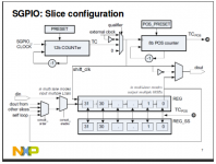
"SCK master mode: SCK is supplied at pin 8, this clock falling edge is used as shift clock for all slices. No MCK is used."
The PRESETi is "counter not used" (it says not value zero) whereas for slice D in MCK master mode PRESET is set to 3: f=MCK/4, but then the other slices are set to use "SGPIO_MUX_CFGi / ext_clk_enable = 0 :internal clock" mapped to slice D in slice mode.
PRESET documentation:
"Each register contains the reload value for one slice: PRESET0 to PRESET15 contain the reload value for slice A (register 0) to slice P (register 15).
This register controls the internally generated slice shift clock frequency: frequency(shift_clock) = frequency(SGPIO_CLK) / (PRESET+1)."
Now is this setting only available for internal clocks (meaning SGPIO_CLK or slice clock)? The slice D on the other hand uses PRESET value 3 (/4) and seems to be configured similarly as SCK otherwise so it seems it could work.
Yeah, figures 42 and 43 in the LPC43xx manual kind of disagree about how clocking works. 19.6.3 is pretty specific about CLKGEN_MODE so I suspect figure 43 is unclear in that external clock should read "clk_slice or clk_pin". Probably the manual just picked up some ambiguity around the definition of external clock through edits over time. This suggests PRESET = 3 in table 321 is incorrect---presumably that cell of the table should say not used---and the clock divide is accomplished by loading SGPIO12's shift registers with 11110000b. With an LPC-Link 2 in hand it's easy enough to check this with a function generator on SGPIO13 and an oscilloscope/logic analyzer/something like that on the outputs.
It is unclear from the manual if a slice can be used if its output is not assigned to a pin, though I don't see any reason why this would be required. So presumably post 543 could be implemented by making SGPIO11 a pin clock to any of SGPIO12 to 15 and then using the chosen slice as a slice clock for the I2S output SGPIOs. Worst case would be pin assignment is required, in which case SGPIO13 would have to be used.
It is unclear from the manual if a slice can be used if its output is not assigned to a pin, though I don't see any reason why this would be required. So presumably post 543 could be implemented by making SGPIO11 a pin clock to any of SGPIO12 to 15 and then using the chosen slice as a slice clock for the I2S output SGPIOs. Worst case would be pin assignment is required, in which case SGPIO13 would have to be used.
It's clear from the Fig. 43 in User Manual that the PRESET does not affect to external clock, just to SGPIO_CLOCK. Wonder what the pre-divider discussed here does mean:
SGPIO with DMA | www.LPCware.com
SGPIO with DMA | www.LPCware.com
Attachments
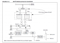
My reading is predivider = PRESET. For the configuration we're discussing here a DMA request can be raised by I2S0 each time a sample is received (section 43.7.3) and it's desirable to use SGPIO14 or 15 to do the same each time a sample is sent and the shift registers exchanged on I2S_SDO_x. In the default I2S case of 32 bits per sample this should be straightforward to implement by operating one of the GPDMA slices in self loop from the SCK slice clock. The default pattern of 0x4000 0000 mentioned in section 19.7.6 should be fine.
However, I think this approach is limited to stereo receive or stereo send. If I'm reading the manual correctly it doesn't work so well with multichannel audio as SGPIO14 and 15 are the only SGPIO destinations available (table 327 got glossed over in post 57 of this thread). One of those needs to be loaded with the pattern to trigger DMA, meaning only the other is available as a DMA destination peripheral. This is fine if the DAC is in one line mode but problematic when operating two or more I2S_SDO lines in parallel as only one line can be a DMA recipient.
Presumably multichannel data is moved via the combined SGPIO interrupt which fires when a slice's REG and REG_SS shift registers are exchanged. This seems to be variously referred to as the capture clock interrupt, exchange clock interrupt, FIFO full interrupt, and POS interrupt depending on which part of the manual one's looking at. Since all I2S_SDO lines exchange registers in sync with I2S_WS the result should be just one interrupt per batch of left or right samples whose handler copies the next 32 bit word to each REG_SS in use.
So, upon closer inspection, it may be desirable to leave U3 and U4 in their default directions on the LPC-Link 2. This enables the configuration below, which supports implementation of a 8 in, 6 out USB audio interface at the I2S level (it's not hard to make the marketing numbers higher---14 in 28 out would be fairly easy, for example).
I2S_IN0
If the I2S0 peripheral is not needed then the single connection to J4 can be omitted and J3 pin 3 used as GP_CLKIN. In this configuration SGPIO9 is freed for use as I2S_IN1_SD3 as SGPIO13 can generate I2S_OUT_SCK through division of CLK_PERIPH_SGPIO. This would most likely occur with an eight channel ADC to, for example, mic a drum kit.
As usual for SGPIO the above pin assignments are tweakable. Most notably, SGPIO14 can be reassigned as an output if 6 in 8 out is preferable. Handy for quadamping.
Disclaimer: I've checked the above in the LPC-Link 2 pinout spreadsheet I've built up but might have made a mistake. Or missed a typo in putting together this post.
I2S_IN0
- J3 pin 3 - I2S0_RX_SCK
- J3 pin 11 - I2S0_RX_WS
- J3 pin 12 - I2S0_RX_SDA
- J8 pin 12 - SGPIO8 - I2S_IN1_SCK - pin clock for rest of I2S_IN1
- J8 pin 14 - SGPIO0 - I2S_IN1_WS
- J8 pin 16 - SGPIO1 - I2S_IN1_SD0
- J8 pin 18 - SGPIO2 - I2S_IN1_SD1
- J8 pin 20 - SGPIO3 - I2S_IN1_SD2
- J4 pin 16 - SGPIO9 - MCLK - yields 128fs pin clock to slice 15
- J3 pin 5 - SGPIO10 - I2S_OUT_WS
- J3 pin 6 - SGPIO13 - I2S_OUT_SCK - clocked from slice 15, yields 64fs slice clock for rest of I2S_OUT
- J8 pin 4 - SGPIO11 - I2S_OUT_SD0
- J8 pin 8 - SGPIO12 - I2S_OUT_SD1
- J8 pin 10 - SGPIO14 - I2S_OUT_SD2 - or J8 pin 2 if U7 is used
If the I2S0 peripheral is not needed then the single connection to J4 can be omitted and J3 pin 3 used as GP_CLKIN. In this configuration SGPIO9 is freed for use as I2S_IN1_SD3 as SGPIO13 can generate I2S_OUT_SCK through division of CLK_PERIPH_SGPIO. This would most likely occur with an eight channel ADC to, for example, mic a drum kit.
As usual for SGPIO the above pin assignments are tweakable. Most notably, SGPIO14 can be reassigned as an output if 6 in 8 out is preferable. Handy for quadamping.
Disclaimer: I've checked the above in the LPC-Link 2 pinout spreadsheet I've built up but might have made a mistake. Or missed a typo in putting together this post.
Yes you could get more I/O using converters supporting TDM (sometime called "DSP") format PCM interface. 8 channel input or output / data line usually (at least if you limit the sample rate to 48kHz, otherwise two lines are required, though there might be exceptions to that). This doesn't apply to I2S I/O pins, but with SGPIO it would be possible.
Btw. I asked Embedded Artist about the TP locations and they wrote this one page document:
http://www.embeddedartists.com/sites/default/files/support/xpr/link2/LPC-Link2_TP-locations.pdf
So if you would like to use the I2S0 which takes the GP_CLKIN signal @J3 pin 3 you could use some of the TP clock inputs supported by CGU (clock gonfig unit) - ENET_TX_CLK (K9) @ TP_P1_19 (or @ TP_CLK if you mux it to K3 pin) pin is one of them.
Yah, hence my comment about there being plenty of ways to get higher IO counts. 6/8 in/out is upper midrange in the interface market. So there's not necessarily need to use I4S, I6S, or I8S (TDM). I happen to have both a Saffire Pro 40 and Scarlett 18i20 at the moment so I'm not exactly short on IOs. The most I use is 5 in 6 out at the moment, though 6 in 8 out might happen if I find a good deal on a C414 and also start using cans/buds and triamped monitors simultaneously.
I do find use of TDM attractive as it allows the 10 SGPIOs on J8 to form three InS links while leaving J3 open for a common MCLK. For example, WM8805 + CS5368 + CS4385 = I2S in+out + I8S in + I8S out = 10 in 8 out. Not bad for plugging a ribbon cable into a USD 20 microcontroller eval board. One can pack the 12 available SGPIOs more tightly to reach for maximum IO (something like 34 in/32 out, not counting MIDI or ADAT) but not requiring common SCKs and WSes ends up being useful for SPDIF or higher end parts. Everything through U4 needing to go the same way gets to be an issue too, so at some point it's easier to do one's own board.
As an aside, it's possible to roll a non-SGPIO I2S in+out on the LPC-Link 2. Goes like this
") I didn't type up the ENET_TX_CLK options in my previous post for two reasons. One is simply brevity. The other is it's probably nicer to tap J4 as that offers better impedance control on the clock net and additional pins for things like a volume pot.
I didn't type up the ENET_TX_CLK options in my previous post for two reasons. One is simply brevity. The other is it's probably nicer to tap J4 as that offers better impedance control on the clock net and additional pins for things like a volume pot.
I do find use of TDM attractive as it allows the 10 SGPIOs on J8 to form three InS links while leaving J3 open for a common MCLK. For example, WM8805 + CS5368 + CS4385 = I2S in+out + I8S in + I8S out = 10 in 8 out. Not bad for plugging a ribbon cable into a USD 20 microcontroller eval board. One can pack the 12 available SGPIOs more tightly to reach for maximum IO (something like 34 in/32 out, not counting MIDI or ADAT) but not requiring common SCKs and WSes ends up being useful for SPDIF or higher end parts. Everything through U4 needing to go the same way gets to be an issue too, so at some point it's easier to do one's own board.
As an aside, it's possible to roll a non-SGPIO I2S in+out on the LPC-Link 2. Goes like this
- J3 pin 3 - I2S0_RX_SCK
- J3 pin 11 - I2S0_RX_WS
- J3 pin 12 - I2S0_TX_SDA
- J9 pin 20 - I2S0_RX_SDA
I didn't type up the ENET_TX_CLK options in my previous post for two reasons. One is simply brevity. The other is it's probably nicer to tap J4 as that offers better impedance control on the clock net and additional pins for things like a volume pot.
Nice chip, also available in TQFP package (64 pin the smallest one). 512 KB RAM. Errata. 300+ DMIPS. PIC32MZ1024ECG064-I/PT-ND $11.57/piece.
XMOS starKIT 1000 MIPS for $14.99 (U16A 2-core - sorry 2-tile, device onboard, first tile boots only from USB though), XS1-L4A-64-TQ48-C4 $4.28/piece (400 MIPS). USB parts only in BGA package.
XMOS starKIT 1000 MIPS for $14.99 (U16A 2-core - sorry 2-tile, device onboard, first tile boots only from USB though), XS1-L4A-64-TQ48-C4 $4.28/piece (400 MIPS). USB parts only in BGA package.
Last edited:
How about the Intel Galileo (board with X1000 SoC)? It does support PCIe so by using an adapter you could run PCIe interface if there are Linux drivers supported. Haven't seen any benchmarks for it's 400 MHz Pentium processor though. Well, might be OT anyway - not embedded enough (well, which OS can be used in this thread anyway, RTOS at least?).
Maybe not worth mentioning but anyway the boards with Cortex-A7 (mentioned in post #46) are coming, there are actually many of them - Olimex A20-OLinuXino, PhoenixA20, Cubieboard2 among the others. At least some of the I2S pins (clocks, data in, 3x data out of 4x outputs) are brought to the external headers. Maybe overkill for the job.
Thanks for pointing this. This is not overkill when grabbing asynchronous audio on USB, while 256-tap FIR filtering six channels, and possibly applying adaptive filtering on the bass channel for keeping within Xmax and thermal limits. And the price is still in the low cost range. This may be the future for inexpensive high-end digital audio processing, from a hardware perspective. On the other hand, from a software perspective, I don't think that Linux or Android are the future for that particular job.Maybe not worth mentioning but anyway the boards with Cortex-A7 (mentioned in post #46) are coming, there are actually many of them - Olimex A20-OLinuXino, PhoenixA20, Cubieboard2 among the others. At least some of the I2S pins (clocks, data in, 3x data out of 4x outputs) are brought to the external headers. Maybe overkill for the job.
Thanks for pointing this. This is not overkill when grabbing asynchronous audio on USB, while 256-tap FIR filtering six channels, and possibly applying adaptive filtering on the bass channel for keeping within Xmax and thermal limits. And the price is still in the low cost range. This may be the future for inexpensive high-end digital audio processing, from a hardware perspective. On the other hand, from a software perspective, I don't think that Linux or Android are the future for that particular job.
Anyone considered multirate filtering, that would make it possible to use also the lesser parts for FIR filtering?
Indeed, but how can you a implement a "bit exact" filter using multirate filtering? You need to decimate, you thus need a lowpass filter, any lowpass filter has a finite slope in frequency domain, any high slope lowpass introduces ringing in time domain, so anyway practically there always will be aliasing. Possibly aggravated by ringing in time domain. This is what most people think about multirate filtering. You may find this quite naive, but that's the current status in 2014.Anyone considered multirate filtering, that would make it possible to use also the lesser parts for FIR filtering?
On the other hand, multirate filtering opens the door to the idea of designing a system having an intrinsic, natural geometric frequency resolution complying with the musical harmony theory.
In such context, a conventional 2-way multirate filtering appears as the worst application. Such 2-way crossover would operate at Fs/16 in the frequency range 0 Hz - Fs/32 (lowpass section) and would operate at Fs in the frequency range Fs/32 - Fs/2 (highpass section). You may add a "bandpass filler" section having a one-octave bandpass response, dedicated to the transition band, transforming the 2-way filter into a 3-way filter. But, from an aesthetic perspective, or harmony perspective, the fact that such system exhibits a strong discontinuity at Fs/32 (or at F/64 and at F/16 with the bandpass filler) looks terrifying.
Thus, what people would better accept, is a quasi-continuous geometric frequency scaling as pre-processor, then filtering (in time-domain and/or in frequency-domain) within such geometric frequency scaling, then applying an inverse geometric frequency scaling as post-processor, just before the output. This way, the lower the frequency, the sharper the frequency resolution from a filtering perspective, intrinsically and progressively. Without any abrupt discontinuity.
What would be the name for something like this?
Can it be computational-effective?
Can the aliasing products and distortions remain under the -96 dB baseline, practically, only sacrificing one ARM core for audio, on a quadcore (MTK6582) or octacore (MTK6592) ARM chip?
steph, try googling :
Frequency-Warped Signal Processing for Audio
Warped Filters
frequency warped FIR
There is - or was - the nwfiir software suite which also used WFIR:
nwfiir audio tools
Last time I tried it didn't compile on gcc version 4.6.3 anymore.
I'm looking to implement an active xover for a multi-channel (home theatre) system, to replace a stack of noisy DCXs. Has anyone looked at using the ADS1278 as an input for such processing? It seems simpler than stacking up a whole pile of stereo ADCs.
The other neat possibility is that you can buy an evaluation module for ~$150 which has the chip on a PCB ready to go, plus a motherboard for testing purposes. Seems to me that this eval board, plugged into one's own DSP motherboard, would be a good front end; all you need to add is a line buffer for each channel.
The only drawback that I see is that the output is not quite I2S. It has 8 data lines for the 8 channels, a bit clock and a frame-sync line. It's like DSP-mode I2S with one channel per line instead of two, if that makes any sense. It'd be fine if you're plugging it into an FPGA as I intend to, but high speed hardware inputs to a DSP might be a problem unless you want to program up a little CPLD to bit-shuffle it into 4 I2S streams.
Any thoughts/objections to its sound quality? Suggestions for better 8-channel ADCs that will do 24/96?
- Status
- This old topic is closed. If you want to reopen this topic, contact a moderator using the "Report Post" button.
- Home
- Source & Line
- Digital Line Level
- Open Source DSP XOs