This talk of codec strapping got me curious so I got to checking back on things. Unsurprisingly, it remains there are no suitable Arduino or Raspberry Pi boards (unsurprisingly, Raspy Fi is still USB out). The BeagleBone Black brings out a full set of mcasp0 pins from its AM3359 to the expansion headers but unfortunately fails to do so in a way that's I2S friendly. Specifically, use of all four AXR pins requires IO mode 3 or 6. But from what I can tell the only mode that sort of works with the user accessible pins on the Black is mode 0, which yields one data line out to the expansion headers whose clocks are shared with the I2S over to HDMI.
I2C and clocks are on the expansion headers, though. So, given a DAC with a one line mode, one could use a Black DAC cape to enable USB -> DSP XO + EQ -> DAC. But not SPDIF -> DSP -> DAC as there's no support for a second data line in mode 0. Enough nets on the board go through resistors one could probably blue wire something up for mode 3 or 6 given a pair of hot tweezers but, eh, it's not something I consider worth the hassle.
I2C and clocks are on the expansion headers, though. So, given a DAC with a one line mode, one could use a Black DAC cape to enable USB -> DSP XO + EQ -> DAC. But not SPDIF -> DSP -> DAC as there's no support for a second data line in mode 0. Enough nets on the board go through resistors one could probably blue wire something up for mode 3 or 6 given a pair of hot tweezers but, eh, it's not something I consider worth the hassle.
hi twest820, thinking about an "audio cape" for the Embedded Artists LPCLINK2?
The Rev. C schematics are here : http://www.embeddedartists.com/sites/default/files/support/xpr/link2/LPC-Link-II_Rev_C.pdf
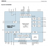
The CPU is a LPC4320, the datasheet says it features Cortex-M4 + Cortex-M0 + SGPIO.
Check J3, J4 and J9 on LPCLINK2 schematic, page 6.
Basically, Embedded Artists say LPCLINK2 it is a standalone debug probe, designed to connect on Embedded Artists LPCXPRESSO boards as targets.
However, J3, J4 and J9 appear to be designed, for LPCKINK2 becoming a target equipped with a "cape" dealing with SGPIO, SSP1, UART2 and I2C.
Now comes the question : how would you debug this? Get a second LPCLINK2 used as debug probe, outputting the SWD lines to the second LPCLINK2 used as target?
The Rev. C schematics are here : http://www.embeddedartists.com/sites/default/files/support/xpr/link2/LPC-Link-II_Rev_C.pdf
The CPU is a LPC4320, the datasheet says it features Cortex-M4 + Cortex-M0 + SGPIO.
Check J3, J4 and J9 on LPCLINK2 schematic, page 6.
Basically, Embedded Artists say LPCLINK2 it is a standalone debug probe, designed to connect on Embedded Artists LPCXPRESSO boards as targets.
However, J3, J4 and J9 appear to be designed, for LPCKINK2 becoming a target equipped with a "cape" dealing with SGPIO, SSP1, UART2 and I2C.
Now comes the question : how would you debug this? Get a second LPCLINK2 used as debug probe, outputting the SWD lines to the second LPCLINK2 used as target?
Last edited:
This talk of codec strapping got me curious so I got to checking back on things. Unsurprisingly, it remains there are no suitable Arduino or Raspberry Pi boards (unsurprisingly, Raspy Fi is still USB out). The BeagleBone Black brings out a full set of mcasp0 pins from its AM3359 to the expansion headers but unfortunately fails to do so in a way that's I2S friendly. Specifically, use of all four AXR pins requires IO mode 3 or 6. But from what I can tell the only mode that sort of works with the user accessible pins on the Black is mode 0, which yields one data line out to the expansion headers whose clocks are shared with the I2S over to HDMI.
I2C and clocks are on the expansion headers, though. So, given a DAC with a one line mode, one could use a Black DAC cape to enable USB -> DSP XO + EQ -> DAC. But not SPDIF -> DSP -> DAC as there's no support for a second data line in mode 0. Enough nets on the board go through resistors one could probably blue wire something up for mode 3 or 6 given a pair of hot tweezers but, eh, it's not something I consider worth the hassle.
Thanks for that I've been toying with the idea of BB(Black)+DIX9211 (I've got an old white BB here at the moment) and need to dig through the pin outs a bit more thoroughly yet to see how that'll work, I'm still pretty new to embedded dev and the datasheets have taken some work to get my head around.
i2s interface on the fpga + linux drivers for a zynq chip still seems the most robust idea though, especially for multichannel i2s.
[Edit for steph's edit.] Only if one uses a generous interpretation of designed. There's no SGPIOs and only part of an I2S route to J9. With only two SGPIO's J4's not useful for audio on its own and the TRACEDATA pins on J8 are only available as SGPIOs if you hack the debug connector to 10 pin Cortex from 20 pin JTAG. J3 has three SGPIOs, I2C, and CLKIN. One could biamp from J3+J4 and triamp/quadamp from J3+J4+J8 but I wouldn't consider either option particularly attractive.However, J3, J4 and J9 appear to be designed, for LPCKINK2 becoming a target equipped with a "cape" dealing with SGPIO, SSP1, UART2 and I2C.
Last edited:
For some reason DIYA's no longer allowing spreadsheets to be attached to posts but if you PM me your email I'll send you my BeagleBone Black spreadsheet extracted from the csv files underlying TI's PinMux tool. Then you can plug the Black's expansion header pins into PinMux and see the mcasp0 IO set violation light up.need to dig through the pin outs a bit more thoroughly yet to see how that'll work
")
PM sent
Xmos have got a new product today, designed in partnership with Silicon Labs Cortex M3 SoC with their programmable logic cores on one chip.
XMOS creates the next wave in programmable system-on-chip products | XMOS
Xmos have got a new product today, designed in partnership with Silicon Labs Cortex M3 SoC with their programmable logic cores on one chip.
XMOS creates the next wave in programmable system-on-chip products | XMOS
Yeah, I was looking at those last night. The M3 addition certainly moves them closer to this thread's definition of open and makes sense from the standpoint of not needing to dedicate an XMOS core to IO. But I find it's hard to get excited about the XMOS cores. 8 16 bit-ish cores at 400MHz to do 20 biquads at 48k is the equivalent of a single M4 at something like 75MHz. And the parts cost around twice as much as M4s for comparable oomph. Fairly woeful compared to a Blackfin as well. On the plus side the tools are free, the eval boards are mostly pretty inexpensive, and there's good LQFP availability.
Interesting - but hard work cutting through the marketing gloss to uncover what's really going on. For example 'programmed completely in C-code'. When I looked at XMOS they had their own version of C called 'XC' - which includes extensions to normal C to handle the concurrency. If this is still the case then this claim is at best misleading as the ARM version of C doesn't support those concurrency constructs. How will developing with two incompatible versions of C pan out I wonder?
Lower down there's the claim that the new SoC will have '8 32-bit processors' which is immediately contradicted by '7 xCore logical cores plus one ARM M3' (italics my own). A logical core and a physical processor look to me to be quite different beasts. Even Intel, rather notorious for reality stretching in its marketing, doesn't say a logical core counts as a physical CPU when promoting its hyperthreading feature. Then the future products with '6-core and 8-core' don't really make sense as they've just described the first one which has already 8 cores.
An interesting thread (pun intended) running through this brief is the use of 'energy' rather than power. Perhaps inherited from Energy Micro which Silicon Labs purchased in the summer ($170m). This rather makes me wonder that the power consumption is nothing to get excited about, what their USP is that it can be put to sleep most of the time with low overhead and low leakage current.
Yeah I'm just dipping my toe in the water and seeing what's around, this thread is a great learning ground for these things, thanks to everyone who has contributed, I've learned stacks! I've got an original BeagleBone and a Parallela on pre-order (Xilinx Zynq 7020 + 16core Adapteva Epiphany III) that I'm hoping to get later in the year ... I'm more comfortable building something that runs inside of Linux so that's where my head is at really. The Epiphany chip is just a nice to have really, I'm more excited to play with the Zynq, the programming of the Epiphany is a bit over my head at the moment though in time I'd like to learn that too and see how far I can get with it. While the runs are small the Epiphany chips look pretty expensive for designing your own boards too. ($US595 for 8 processors ... not really DIY friendly at this stage)
The whole big.LITTLE architecture is also of interest for running this stuff inside Linux too, though I note that's really not where this thread is going ... sorry for offtopic ...
The whole big.LITTLE architecture is also of interest for running this stuff inside Linux too, though I note that's really not where this thread is going ... sorry for offtopic ...
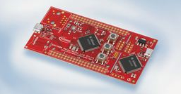
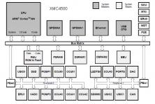
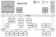
Let's see how a WM8580 "multichannel audio codec cape" would connect on the XMC4500 Relax Lite Kit available from HITEX, costing 10 euro (without shipment and tax).
The WM8580 cape would feature a local quartz, connected to the WM8580.
The WM8580 features an internal PLL generating all audio clocks, including MCLK.
The WM8580 would act as I2S master, sending the I2S bit_clock and I2S frame_sync to the XMC4500.
Consequently, the XMC4500 doesn't see MCLK.
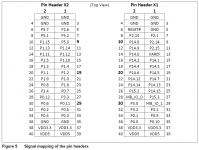
Viewed from the XMC4500 Relax Lite Kit :
Pin Header X2 delivers :
- two full-duplex I2S (slaves)
- one SPI (master)
Pin Header X1 delivers :
- one full-duplex I2S (slave)
It could be that hacking pin 17 and pin 19 on IC200 footprint, one may get as extra :
- one I2C
Thus, the XMC4500 Relax Lite Kit + WM8580 cape would implement a stereo 3-way Xover :
- taking one I2S as input (audio may come from the WM8580 SPDIF-in, or from the WM8580 stereo ADC)
- delivering three I2S as outputs (six line-level analog channels out).
Volume control would be done using the WM8580 output level registers.
There could be a connector for adding an external high quality multichannel volume control, such connector carrying SPI plus chip select, or I2C.
Asynchronous USB audio could come later on, using a second "cape" featuring a second XMC4500 dedicated to the USB protocol, requesting stereo audio samples with the same WM8580 still acting as local, master audio clock and multichannel DAC. One could add galvanic isolation at this stage.
What's your opinion about this?
The WM8580 cape would feature a local quartz, connected to the WM8580.
The WM8580 features an internal PLL generating all audio clocks, including MCLK.
The WM8580 would act as I2S master, sending the I2S bit_clock and I2S frame_sync to the XMC4500.
Consequently, the XMC4500 doesn't see MCLK.
Viewed from the XMC4500 Relax Lite Kit :
Pin Header X2 delivers :
- two full-duplex I2S (slaves)
- one SPI (master)
Pin Header X1 delivers :
- one full-duplex I2S (slave)
It could be that hacking pin 17 and pin 19 on IC200 footprint, one may get as extra :
- one I2C
Thus, the XMC4500 Relax Lite Kit + WM8580 cape would implement a stereo 3-way Xover :
- taking one I2S as input (audio may come from the WM8580 SPDIF-in, or from the WM8580 stereo ADC)
- delivering three I2S as outputs (six line-level analog channels out).
Volume control would be done using the WM8580 output level registers.
There could be a connector for adding an external high quality multichannel volume control, such connector carrying SPI plus chip select, or I2C.
Asynchronous USB audio could come later on, using a second "cape" featuring a second XMC4500 dedicated to the USB protocol, requesting stereo audio samples with the same WM8580 still acting as local, master audio clock and multichannel DAC. One could add galvanic isolation at this stage.
What's your opinion about this?
Attachments
Last edited:
The whole big.LITTLE architecture is also of interest for running this stuff inside Linux too, though I note that's really not where this thread is going ... sorry for offtopic ...
The LPC43XX seems to me to be the original big.LITTLE instantiation so the architecture is very much on topic. Linux already has a thread of its own somewhere. Myself I veer much more towards the 'bare-metal' approach of doing the most with the fewest resources. If NXP had put a decent serial port (even an SSP) on their M0+ offering (LPC8XX) I'd even be drooling over that for simple DSP - as it is it looks possibly only useful for programming up stuff that needs I2C comms. Perhaps though I need to dig deeper into how to get the most out of the SPI....
I must agree! Tell me, if the Infineon XMC4500 was branded NXP, you would already have designed a "digital audio cape" for the Relax Lite Kit, isn't ? In other words, what do you dislike in the Infineon XMC4500?If NXP had put a decent serial port (even an SSP) on their M0+ offering (LPC8XX) I'd even be drooling over that for simple DSP...
I would say yes. See the attached screenshot from Digi-Key. Quite amazing, the XMC4500 Relax Lite Kit from Hitex (10.00 eur = 13.80 dollar) is about the same price as one bare XMC4500 chip from Digi-Key (13.60 dollar). However, the XMC4500 Relax Lite Kit from Hitex embeds two XMC4500 chips : one for the breakable programmer/debugger, and another for the target. Let's hope the XMC4500 price is going to significantly drop. This reminds me the very first STM32F4 prices, about 15 dollar. Now you can buy STM32F4 versions for 11 dollar.Is XMC4500 fully available now?
Attachments
Last edited:
From a quick look through the DS - its just a bit complex as a starter M4 chip for me, and rather power hungry at around 100mA. Much more suitable for my current needs is the 4100, with 24mA Isupply and fewer pins on the packages. It really reminds me of the TI M4s (uncanny that its also 80MHz) which never really arrived. Is it available and what's the price?
STM32Fs are still too expensive for what they are. Freescale and NXP are better value although NXP lacks a real low-end M4.
STM32Fs are still too expensive for what they are. Freescale and NXP are better value although NXP lacks a real low-end M4.
Very nice finding, kind of poor man's XMC4500. Only two USICs. Let's try the following XMC4100 USIC allocation :Much more suitable for my current needs is the XMC4100, with 24mA Isupply and fewer pins on the packages. Is it available and what's the price?
- U0C0 as SPI master (controlling Codec registers etc.)
- U0C1 as I2S
- U1C0 as I2S
- U1C0 as I2S
This way we get a stereo 3-way crossover (6 analog line out), something a STM32F4 can't implement (it only features two I2S).
Unfortunately, the XMC4100, XMC4200 and XMC4400 are not yet available.
Currently, the only available parts within the XMC4000 family are the XMC4500. They feature three USICs.
Attachments
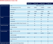
OK steph, you got me interested in the XMC4XXX range now. For the parts that are so far unavailable, there does look to be a whole wealth of information provided. NXP doesn't tell you power supply currents until they've actually got parts to characterize, so I'm betting these parts do actually exist and are in some privileged customers' hands. There are even errata sheets for the 4100, looks like they've had three die revs so far and the latest is no longer at 'ES'.
I note that the 4400 has nice 64pin packages and goes up to 120MHz, albeit with rather higher supply current.
I note that the 4400 has nice 64pin packages and goes up to 120MHz, albeit with rather higher supply current.
Here's something to get you guys going.
This dude has been selling TMS320 boards for a while on ebay so it is a well established product by the looks of it. This one runs at 150MHz and does floating point if need be. It has 2 McBSP ports which means a total of 4x I2S channels or stereo 4 way active crossover. JTAG ICE's are cheap at about $50-60 and TI stuff is very well documented and supported.
TMS320F28335PGFA Package 176 LQFP Development Board TI DSP | eBay
Chip data can be found at C2000 32-bit Real-time Control MCUs - C28x Delfino Floating-point MCUs - TMS320F28335 - TI.com
All it needs is someone to design a ADC/DAC addon board etc. Sounds like a job for you abraxiloto
- Status
- This old topic is closed. If you want to reopen this topic, contact a moderator using the "Report Post" button.
- Home
- Source & Line
- Digital Line Level
- Open Source DSP XOs